NSA Backdoor Part 2, BULLDOZER: And, Learn How to DIY a NSA Hardware Implant
This article is the second part of a series on NSA BIOS Backdoor internals. This part focuses on BULLDOZER, a hardware implant acting as malware dropper and wireless communication "hub" for NSA covert operations. Despite that BULLDOZER is a hardware, I still use the word "malware" when referring to it because it's a malicious hardware. Perhaps the term "malware" should refer to both malicious software and malicious hardware, instead of referring only to the former.
I'd like to point out why the BULLDOZER is classified as "god mode" malware. Contrary to DEITYBOUNCE, BULLDOZER is not a name in the realms of "gods". However, BULLDOZER provides capabilities similar to "god mode" cheat in video games—which make the player using it close to being invincible—to its payload, GINSU. Therefore, it's still suitable to be called god mode malware. The presence of BULLDOZER is very hard to detect, even with the most sophisticated anti malware tool during its possible deployment timeframe. As for GINSU, we will look into GINSU in detail in the next installment of this series.

Get your free course catalog
The NSA ANT Server document—leaked by Edward Snowden—describes BULLDOZER briefly. This article presents an analysis on BULLDOZER based on technical implications of the information provided by the NSA document. Despite lacking in many technical details, we could still draw a technically-sound analysis on BULLDOZER based on BIOS and hardware technology on the day BULLDOZER became operational, just like in the DEITYBOUNCE case. :-)
Introduction to GINSU-BULLDOZER Malware Combo
BULLDOZER doesn't work in isolation. It has to be paired with the GINSU malware to be able to work. As you will see in the next installment of this article, GINSU is a malicious PCI expansion ROM. Therefore, at this point, let's just assume that GINSU is indeed a malicious PCI expansion ROM and BULLDOZER is the hardware where GINSU runs. This means BULLDOZER is a PCI add-in card, which is in line with the information in the NSA ANT server document.
Before we proceed to analyze BULLDOZER, let's look at the context where BULLDOZER and GINSU work. GINSU and BULLDOZER are a software and hardware combo that must be present at the same time to work. We need to look at the context where GINSU and BULLDOZER operate in order to understand their inner working. Figure 1 shows the deployment of GINSU and BULLDOZER in the target network.
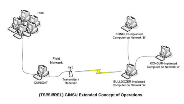
Figure 1 GINSU Extended Concept of Operations. Courtesy: NSA ANT Product Data
Figure 1 shows BULLDOZER hardware implanted in one of the machines in the target network. The NSA Remote Operation Center (ROC) communicates via OMNIGAT with the exploited machine through an unspecified wireless network. This implies the GINSU-BULLDOZER malware combo targets machines in air-gapped networks or machines located in a network that is hard—but not impossible—to penetrate. In the latter case, using machines with malware-implanted hardware is more economical and/or stealthier compared to using an "ordinary" computer network intrusion approach.
Let's look closer at the technical information revealed by the NSA ANT product data document, before we proceed to deeper technical analysis. The NSA ANT server product data document mentions:
- GINSU provides software application persistence for the Computer Network Exploitation (CNE) implant—codenamed KONGUR—on systems with the PCI bus hardware implant, BULLDOZER.
- The technique supports any desktop PC system that contains at least one PCI connector (slot) and uses Microsoft Windows 9x, 2000, 2003 server, XP, or Vista. The PCI slot is required for the BULLDOZER hardware implant installation.
- BULLDOZER is installed in the target system as a PCI hardware implant through "interdiction"—fancy words for installing additional hardware in the target system while being shipped to its destination.
- After fielding, if KONGUR is removed from the system as a result of operating system upgrade or reinstallation, GINSU can be set to trigger on the next reboot of the system to restore the software implant.
It's clear that there are three different components in the GINSU-BULLDOZER combo from the four points of information above and from Figure 1. They are as follows:
-
The first component is GINSU. The GINSU code name is actually rather funny because it refers to a knife that was very popular in 1980s and 1990s via direct sell marketing. Perhaps the creator of the GINSU malware refers to the Ginsu knife's above average capability to cut through various materials. GINSU is possibly a malicious PCI expansion ROM—PCI expansion ROM is also called PCI option ROM in many PCI-related specifications; I will use both terms in this article. GINSU might share some modules with DEITYBOUNCE because both are a malicious PCI expansion ROM—see the DEITYBOUNCE analysis at https://www.infosecinstitute.com/resources/malware-analysis/nsa-bios-backdoor-aka-god-mode-malware-part-2-bulldozer/.
However, it differs in many other aspects. First, GINSU runs on the NSA custom PCI add-in card, codenamed BULLDOZER. Therefore, GINSU could be much larger in size compared to DEITYBOUNCE because NSA controls the size of the flash ROM on the PCI add-in card. This means GINSU could incorporate a lot more functions compared to DEITYBOUNCE. Second is the type of PCI add-in card type that GINSU might use. From Figure 1, GINSU hardware (BULLDOZER) seems to masquerade as a WLAN PCI add-in card or other kinds of PCI add-in cards for wireless communication. This implies the PCI class code for the BULLDOZER hardware that contains GINSU probably is not a PCI mass storage controller like the one used by DEITYBOUNCE. Instead, the BULLDOZER PCI chip very possibly uses a PCI wireless controller class code.
-
The second component is named BULLDOZER. This codename perhaps refers to the capability of BULLDOZER to push large quantities of materials to their intended place, which in the context of GINSU provides the capability to push the final payload (KONGUR) to the target systems. In this particular malware context, BULLDOZER refers to the PCI add-in card (hardware) implant installed in the target machine. BULLDOZER is a custom PCI add-in card. It very probably masquerades as a PCI WLAN add-in card because it provides a wireless communication function that requires a certain kind of antenna. However, this doesn't prevent BULLDOZER from masquerading as another kind of PCI add-in card, but the presence of a physically larger antenna in the PCI WLAN card could boost the wireless signal strength. Therefore, the NSA might use the PCI WLAN card form factor to their advantage. We will look deeper into BULLDOZER implementation later.
- The third (last) component is named KONGUR. KONGUR is a bit mysterious name. It may refer to Kongur Tagh Mountain in China's Xinjiang-Uyghur Autonomous Region. This could possibly means that the GINSU-BULLDOZER combo was devised for a campaign to infiltrate Chinese computer systems. After all, the Xinjiang-Uyghur Autonomous Region is famous for its people's rebellion against the Chinese central government. This doesn't mean that the GINSU-BULLDOZER combo wasn't used against other targets in other campaigns though. KONGUR is a Windows malware that targets Windows 9x, 2000, XP, Server 2003 and Vista. GINSU provides the delivery and reinstallation mechanism for KONGUR. We can view KONGUR as the payload of the GINSU-BULLDOZER combo. It's possible that KONGUR could also work in Windows Vista derivatives, such as Windows 7 and Windows Server 2008, or even later Microsoft operating system (OS), such as Windows 8, Server 2012, and 8.1 because KONGUR also targets Windows Vista, and we don't know which 0-day exploit it uses and whether the 0-day exploit has already been patched or not.
This article doesn't delve deep into KONGUR and GINSU; the focus is on its hardware delivery mechanism, the BULLDOZER malware. The GINSU-BULLDOZER malware combo is the second NSA BIOS malware that we looked into that "abuses" the PCI expansion ROM—after DEITYBOUNCE. Well, we could say that the NSA is quite fond of this technique. Though, as you will see later, it's a justified fondness. Anyway, this hypothesis on the GINSU-BULDOZER combo is bound to have subtle inaccuracies because I have no sample of the malware combo to back-up my assertions. I'm very open to constructive criticism in this regard.
Now, we are going to look into BULLDOZER technical details. However, if you're not yet familiar with the PCI bus protocol, please read the first part of this series (https://www.infosecinstitute.com/resources/malware-analysis/nsa-bios-backdoor-aka-god-mode-malware-part-2-bulldozer/). There are links in that article that further break down the required prerequisite knowledge, just in case you're not up to speed yet.
BULLDOZER: NSA Malicious PCI Add-In Card
In this section we delve into details of the procedures that the NSA probably carries out to create the BULLDOZER hardware implant. Surely, the exact type of hardware used by the NSA may very well be different. However, I try to draw the closest analogy possible from the public domain knowledge base.
Despite the NSA's superiority compared to the private sectors, all of us are bound to the laws of physics and must adhere to hardware protocol in the target systems. Therefore, the NSA's approach to build BULLDOZER couldn't be that much different than the explanation in this article. In the BULLDOZER Implementation Recap section, I try to draw the most logical hypotheses on the BULLDOZER hardware implant, based on the explanation of the process in designing and creating a PCI add-in card similar to BULLDOZER.
PCI add-in cards are installed on PCI expansion slots on the motherboard. Figure 2 shows a PCI add-in card sample. This PCI add-in card is a PCI WLAN card. Figure 2 highlights the PCI "controller" chip from Ralink—a WLAN controller—and the PCI slot connector in the add-in card. The term "controller" is a generic name given to a chip that implements the core function in a PCI add-in card. PCI hardware development documentation typically uses this term, as do PCI-related specifications.
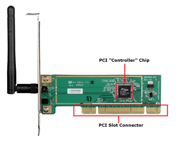
Figure 2 PCI add-in card sample. Courtesy: D-Link.
I use a PCI WLAN card as an example because the GINSU extended concept of operation implies that the BULLDOZER hardware implant is a PCI wireless controller card. As to what kind of wireless protocol it uses, we don't know. But, the point is, BULLDOZER could masquerade as a PCI WLAN card for maximum stealth. It would look innocuous that way. Figure 2 doesn't show the presence of any flash ROM in the PCI add-in card. The PCI add-in card typically stores the PCI option ROM code in the flash ROM. The purpose of Figure 2 is just to show you the typical appearance of the PCI add-in card for wireless communications. We'll get into the flash ROM stuff later on.
PCI Add-In Card in OEM Desktop PC Circa 2008
Now, let's look at how a typical 2008 desktop PC could be implanted with such a card. One of the desktop PCs from a system builder that still had a PCI slot(s) in 2008 is the Lenovo ThinkCentre M57 Desktop PC. I chose a Lenovo desktop PC as an example because its products were widely used in China—besides other parts of the world. It could probably be one of the victims of the GINSU-BULLDOZER campaign. Who knows? The Lenovo ThinkCentre M57 has two PCI slots. Let's say NSA "interdicts" such a system. They can install BULLDOZER in it and then replace the user guide as well to make the BULLDOZER implant look like a legitimate PCI add-in card that comes with the PC, just in case the user checks the manual before using the system.
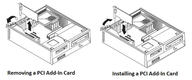
Figure 3 Lenovo ThinkCentre M57 PCI Add-In Card Replacement Instructions (edited version of the original ThinkCentre Hardware Maintenance Manual instructions). Courtesy: Lenovo.
The Lenovo ThinkCentre Hardware Maintenance Manual even comes with instructions to replace a failed PCI add-in card. Figure 3 shows the instruction to replace a PCI add-in card in an "exploded view" style. Hardware replacement instructions shown in Figure 3 are a pedestrian task to do; any NSA field agent can do that.
PCI Wireless Communication Add-In Card Hardware and Software Co-Development
Now, let's look at the steps to develop a PCI wireless communication add-in card in general, because we presume that BULLDOZER falls within this PCI add-in card category. I'm quite sure the NSA also follows the approach explained here, despite being a very advanced spying agency. Only the tools and hardware it uses are probably different—perhaps custom-made.
From a cost point of view, using a Commercial Off-The-Shelf (COTS) approach in creating BULLDOZER hardware would be more cost-effective, i.e. using tools already in the market cost much less than custom tools. COTS benefited from economic of scale and competition in the market compared to custom tools. Moreover, from operational standpoint, the GINSU-BULLDOZER target systems would likely evolve after five years, which dictates the use of new tools. Therefore, obsolescence, which usually plagues COTS solutions, is not a problem in the GINSU-BULLDOZER campaign. The latter fact strengthened my suspicion that the NSA very probably uses the COTS approach. We'll look at this COTS approach shortly.
The "crude" steps to develop a PCI add-in card and its assorted software in general—via the COTS approach—are as follows:
-
High-level design. This step involves the high-level decision on what kind of PCI controller chip would be created for the PCI add-in card and what features the chip would implement and what auxiliary support chip(s) are required. For example, in the case of a PCI wireless communication add-in card, typically you will need a separate Digital Signal Processor (DSP) chip, or you need to buy the DSP logic design from a DSP vendor and incorporate that design into your PCI Field Programmable Gate-Array (FPGA).
-
Hardware prototyping. This step involves creating the PCI controller chip prototype with a PCI FPGA development board. Typically, the language used to develop the PCI controller chip in the FPGA is either VHDL or Verilog. This mostly depends on the FPGA vendor.
-
Software (device driver) development. This step involves creating a prototype device driver for the PCI add-in card for the target Operating System (OS). For example, if the device would be marketed for mostly Windows users, then creating a Windows device driver would take priority. As for other target OS, it would be developed later or probably not at all if market demands on the alternative OS don't justify the cost involved in developing the driver. This step is typically carried-out in parallel to hardware prototyping once the first iteration of the FPGA version of the chip is available. Some FPGA vendors provide a "template" driver for certain target OS to help with the driver development. This way, the PCI controller chip development can run in parallel with the chip design. There are also third-party "driver template" vendors which are endorsed by the FPGA vendors, such as Jungo Windriver—see http://www.jungo.com/st/products/windriver/.
-
Chip fabrication, also known as the making of the Application Specific Integrated Circuit (ASIC). In this step, the first design revision of the chip is finished and the design is sent to chip fabrication plant for fabrication, such as TSMC, UMC or other contract semiconductor fab. This is an optional step though, because some low-volume PCI add-in cards these days are made out of FPGA anyway. If the cost of chip fabrication doesn't make economic sense against creating the product out of FPGA, then the final product uses FPGA anyway. Well, the NSA has several semiconductor fabs—for example, see http://www.chron.com/news/houston-texas/houston/article/NSA-plant-in-San-Antonio-shrouded-in-secrecy-4604109.php. One of the NSA's fab probably was used to fabricate BULLDOZER PCI controller chip.
- Compatibility test on the PCI hardware-software "combo". The chip vendor carries out the compatibility testing first. If the target OS is Windows, Microsoft also carries out additional compatibility testing. In the Windows platform, there is this so-called "WHQL" testing. WHQL stands for Windows Hardware Quality Labs. Windows Hardware Quality Labs testing or WHQL Testing is Microsoft's testing process which involves running a series of tests on third-party hardware or software, and then submitting the log files from these tests to Microsoft for review. In case the primary target OS is not Windows, only the test from the hardware vendor is carried out. The NSA very probably also carries out this kind of test, but for an entirely different purpose, i.e. to make sure the driver works as stealthily as possible or to mislead the user to think the driver is just an ordinary PCI device driver.
Steps 2 and 3 are actually iterative steps. The PCI hardware prototype goes through several iterations until it matures and is ready for fabrication. Step 4 could also happen as an iterative step, i.e. there are several revisions of the chip. The first revision might have a flaw or performance weakness that must be improved, despite being a functional design. In the commercial world, ASICs typically have several revisions. Each revision is marked as a "stepping". You would find the word "stepping" mentioned in many CPU, chipset or System-on-Chip (SoC) technical documentation.
"Simulating" BULLDOZER Hardware
Now, let's look into the process of developing a specific PCI add-in card, i.e. a PCI add-in card with wireless communication as its primary function. We focus on this kind of PCI add-in card because BULLDOZER connects to the outside world—to OMNIGAT in Figure 1—via an unspecified wireless connection. For this purpose, we look into the hardware prototyping step in more detail. Let's start with some important design decisions in order to emulate BULLDOZER capabilities, as follows:
- The prototype must have the required hardware to develop a custom wireless communication protocol. The reason is because the wireless communication protocol used by BULLDOZER to communicate with OMNIGAT must be as stealthy as possible, despite probably using the same physical antenna as a PCI WLAN card.
- The prototype must have an implemented PCI expansion ROM hardware. The reason is because GINSU is a malicious PCI expansion ROM code that must be stored in a functional PCI expansion ROM chip to work.
- GINSU is configurable, or at the very least it can be optionally triggered—based on the NSA ANT server document. This means there must be some sort of non-volatile memory in the prototype to store GINSU parameters. It could be in the form of a Non-Volatile RAM (NVRAM) chip, like in the DEITYBOUNCE case. Storing the configuration data in a flash ROM or other kinds of ROM is quite unlikely, given the nature of flash ROM which requires a rather complicated procedure to rewrite.
The next step is to choose the prototyping kit for the hardware. There are many PCI FPGA prototyping board in the market. We will look into one of them from Sundance (http://www.sundance.com). Sundance is probably a very obscure vendor to you. However, this vendor is one of the vendors that provide a PCI development board for a Software-Defined Radio (SDR) application. You might be asking, why would I pick a PCI SDR development board as an example? The reason is simple, because SDR is the best approach when you want to develop your own wireless protocol. You can tune the frequency, the type of modulation, transmitter power profile, and other parameters needed to make the protocol as stealthy as possible.
BULLDOZER Hardware "Simulation" with Sundance SMT8096 SDR Development Kit
There are usually more than one FPGA in a typical PCI SDR development board. We are going to look into one of Sundance products which were available in the market before 2008—the year the GINSU-BULLDOZER malware combo was operational. I picked Sundance SMT8096 SDR development kit as the example in this article. This kit was available in the market circa 2005. The kit consists of several connected boards with a "PCI carrier" board acting as the host of all of the connected boards. The PCI carrier board connects the entire kit to the PCI slot in the development PC. Figure 4 shows the entire Sundance SMT8096 SDR development kit hardware.
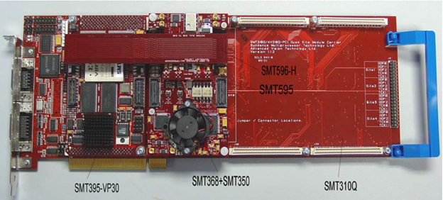
Figure 4 Sundance SMT8096 SDR development kit. Courtesy: Sundance Multiprocessor Technology Ltd.
Figure 4 shows the components of the Sundance SMT8096 SDR development kit. As you can see, the development kit consists of several circuit boards as follows:
Figure 5 shows the block diagram of the entire SDR development kit. It helps to understand interactions between the SDR development kit components.
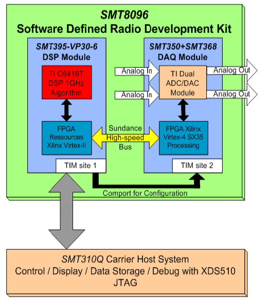
Figure 5 Sundance SMT8096 Development Kit Block Diagram. Courtesy: Sundance Multiprocessor Technology Ltd.
Let's look into SMT310Q PCI carrier board, because this board is the visible one from the motherboard BIOS perspective. We'll focus on the technology required to communicate with the host PC instead of the technology required for the wireless communication, because we have no further clues on the latter. Moreover, I'm not an expert in radio communication technology in anyway.
The SMT310Q PCI carrier board has a QuickLogic V363EPC PCI bridge chip, which conforms to PCI 2.1 specifications. This chip was developed by V3 Semiconductor, before the company was bought by QuickLogic. The V363EPC PCI Bridge connects the devices on the SMT8096 development kit to the host PC motherboard—both logically and electrically—via the PCI slot connector. This PCI bridge chip is not a PCI-to-PCI bridge, rather it's a bridge between the custom bus used in the SMT8096 development kit and the PCI bus in the host PC. The correct term is Local Bus to PCI Bridge. Local bus in this context refers to the custom bus in the SMT8096 development kit—used for communication between the chips in the development kit boards.
At this point we have made the important design decisions, we have picked the PCI hardware development kit to work with, and we have looked into the PCI-specific chip in the development kit. It's time to get into details of the design implementation. The steps to implement the design are as follows:
-
Assuming the wireless communication protocol has been defined thoroughly, the first step is to implement the protocol in the form of DSP chip firmware code and FPGA designs. The DSP chip firmware code consists of initialization code required to initialize the DSP chip itself, code to initialize the interconnection between the DSP chip and the Local Bus to PCI Bridge via the Local Bus interface, and code for other auxiliary functions. Assuming we use the Sundance SMT8096 kit, this step consists of creating the firmware code for the Texas Instrument TIC6416T DSP chip and creating the FPGA designs for the Xilinx Virtex-II and Xilinx Virtex-4 SX35. We are not going to delve into the details of this step, as we don't know the specifics of the wireless communication protocol.
- The second step is to customize the hardware to support the PCI expansion ROM. This is required because we assume the GINSU malware is a malicious PCI expansion ROM code. In this step we configure the SMT310Q carrier board to support the PCI expansion ROM because this board is the one that interfaces with the host (x86/x64 desktop) PCI bus, both at the logical and physical level. We have to enable the Expansion ROM Base Address Register (XROMBAR) in the QuickLogic V363EPC PCI bridge chip (Local Bus to PCI Bridge) in the SMT310Q carrier board via hardware configuration, and we have to provide a flash ROM chip to store the PCI expansion ROM code on the board as well. If you're not familiar with XROMBAR, refer to my Malicious Code Execution in PCI Expansion ROM article (https://www.infosecinstitute.com/resources/hacking/pci-expansion-rom/) for the details.
Now, let's focus on the last step: customizing the hardware required for the PCI expansion ROM to work. It's the SMT310Q carrier board that implements the PCI bus protocol support in SMT8096 PCI SDR development kit. Therefore, we are going to scrutinize the SMT310Q carrier board to find out how we can implement the PCI expansion ROM on it. We start with the board block diagram. Figure 6 shows the SMT310Q block diagram. The block diagram is not a physical block diagram of the board. Instead, it's a logical block diagram depicting logical interconnections between the board components.
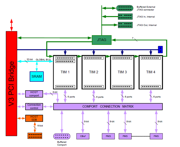
Figure 6 SMT310Q Block Diagram. Courtesy: Sundance Multiprocessor Technology Ltd.
Figure 6 shows blocks marked as TIM, i.e. TIM 1, TIM 2 and so on. TIM is an abbreviation for Texas Instrument Modules. TIM is a standard interconnection between boards using a Texas Instrument DSP chip and other board(s). I couldn't find the latest version of TIM specifications. However, you can find TIM version 1.01 on the net. Despite that TIM implies that a DSP that should be connected via this interconnect, in reality, anything that conforms to the specifications can be connected. It's important to know about TIM, because we are going to use it to "wire" the PCI expansion ROM and also to "wire" NVRAM into the SMT310Q carrier board later.
Figure 6 shows that the QuickLogic V363EPC PCI bridge—marked as V3 PCI Bridge—connects to the TIMs via the 32-bit Global Bus. The 32-bit Global Bus corresponds to the LAD[31:0] multiplexed address and data lines in the QuickLogic V363EPC datasheet. This means the logical and physical connection from QuickLogic V363EPC to the PCI expansion ROM and the NVRAM in our design will be based on the Global Bus.
Now, let's look at how QuickLogic V363EPC exposes devices wired to the TIMs into the host x86/x64 CPU address space. QuickLogic V363EPC uses the so-called "data transfer apertures" to map devices connected through LAD[31:0] into the host x86/x64 CPU address space. These apertures are basically an address range claimed by the PCI Base Address Registers (BARs) in QuickLogic V363EPC. QuickLogic V363EPC datasheet uses different naming scheme for PCI BARs. Figure 7 shows the PCI BARs marked as PCI_BASEx registers. The PCI_MAPx registers in Figure 7 control the amount of memory or I/O range claimed by the PCI_BASEx registers. If you are new to PCI configuration space registers, my Malicious Code Execution in PCI Expansion ROM article (https://www.infosecinstitute.com/resources/hacking/pci-expansion-rom/) has a deeper explanation on the subject. You can compare the "standard" PCI configuration space registers explained there and the ones shown in Figure 7.
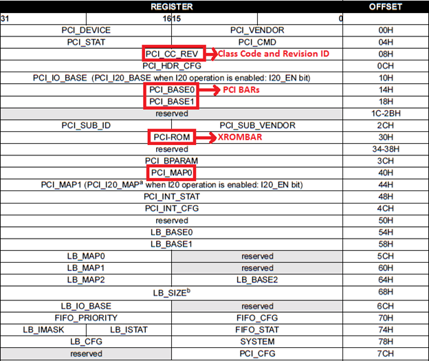
Figure 7 QuickLogic V363EPC PCI configuration registers. Courtesy: QuickLogic V363EPC datasheet.
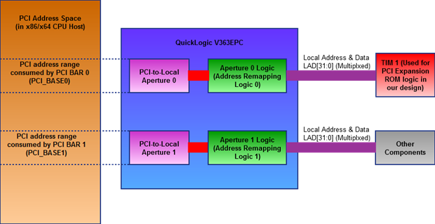
Let's look deeper into the "data transfer aperture" in QuickLogic V363EPC. The "aperture" is basically address remapping logic, i.e. it remaps addresses from the host x86/x64 CPU address space into the local address space in the SMT310Q PCI add-in board. If you're new to address remapping, you can read a sample of the concept in https://www.infosecinstitute.com/resources/reverse-engineering/system-address-map-initialization-x86x64-architecture-part-2-pci-express-based-systems/. Figure 8 shows simplified block diagram of the QuickLogic V363EPC aperture logic (address remapper).
Figure 8 QuickLogic V363EPC Aperture Logic
Figure 8 shows QuickLogic V363EPC claims two different ranges in the PCI address space of the host x86/x64 CPU address space. We are only going to delve into the first range claimed by the PCI_BASE0 register. This is the relevant excerpt from QuickLogic V363EPC datasheet:
"4.1.8 Special Function Modes for PCI-to-Local Bus Apertures
PCI-to-Local bus aperture 0 shares some functionality with the expansion ROM base aperture. The address decoder for PCI-to-Local aperture 0 is shared with the expansion ROM base register. When the expansion ROM base is enabled, the decoder will only bridge accesses within the ROM window. When the ROM is disabled, PCI-to-Local bus aperture 0 will function as described above. Typically, the expansion ROM is used only during BIOS boot, if at all. The expansion ROM base register can be completely disabled via software."
The excerpt above clarifies the PCI expansion ROM mapping. Basically, it says that when the PCI expansion ROM chip mapping is enabled via the XROMBAR register, the aperture will be used only for access to the PCI expansion ROM chip. No other chip can claim the transaction via the aperture.
XROMBAR in QuickLogic V363EPC chip must be enabled in order to support PCI expansion ROM. This is quite a complicated task. We must find the default XROMBAR register value in the chip. The XROMBAR is named PCI_ROM register in QuickLogic V363EPC datasheet, as you can see in Figure 7.
QuickLogic V363EPC datasheet mentions that PCI_ROM (XROMBAR) default value upon power-on is 00h. This means the XROMBAR is disabled because its least significant bit is zero—per PCI specification. However, this is not a problem as the default values of the PCI configuration space registers in QuickLogic V363EPC PCI bridge can be made configurable. There are hardware "straps" that control the default values of the PCI configuration space registers in QuickLogic V363EPC. One of the "straps'" configuration instructs QuickLogic V363EPC to "download" its PCI configuration space registers default values from an external serial EEPROM chip. Pay attention to the fact that this serial EEPROM chip is an entirely different chip from the PCI expansion ROM chip. Figure 9 shows the "straps" option for V363EPC PCI configuration space registers.
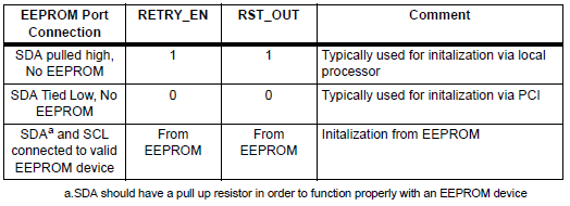
Figure 9 QuickLogic V363EPC PCI Configuration Space Registers Default Values Initialization "straps" Option. Courtesy: QuickLogic V363EPC datasheet.
Figure 9 shows there are two "straps" that control the default value initialization in V363EPC, i.e. SDA and SCL. Both of these "straps" are actually pins on the V363EPC chip. As you can see, when SDA and SCL are connected to serial EEPROM, the PCI configuration space registers default values will be initialized from serial EEPROM. The SDA and SCL pins adhere to I2C protocol. I2C is a serial protocol to connect microcontroller and other peripheral chips in a cost efficient manner, i.e. in as small a number of pins as possible, because pins and traces on a circuit board are costly to design and manufacture. SDA stands for Serial Data and SCL stands for Serial Clock, respectively.
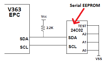
Figure 10 V363EPC to serial EEPROM connection circuit schematic. Courtesy: QuickLogic V363EPC datasheet.
Figure 10 shows the circuit schematic to implement loading default PCI configuration space registers from EEPROM. Now we know how to "force" V3636EPC PCI configuration space registers default values to our liking.
Once the pull-up resistors are set up to configure QuickLogic V363EPC to use serial EEPROM, the QuickLogic V363EPC PCI configuration space registers default values are stored in serial EEPROM and automatically loaded to QuickLogic V363EPC PCI configuration space after power-on or PCI bus reset, prior to PCI bus initialization by the motherboard BIOS. This means we can configure the XROMBAR default value via contents of the serial EEPROM. Therefore, the PCI_ROM (XROMBAR) can be enabled.
Another PCI configuration register to take into account is the PCI_MAP0 register. The PCI_MAP0 register—highlighted in red box in Figure 7—controls whether the PCI_ROM register is enabled or not. It also controls size of the ROM chip to be exposed through the PCI_ROM register. Let's look into details of the PCI_MAP0 register. Figure 11 shows the relevant excerpt for PCI_MAP0 register from QuickLogic V363EPC datasheet.
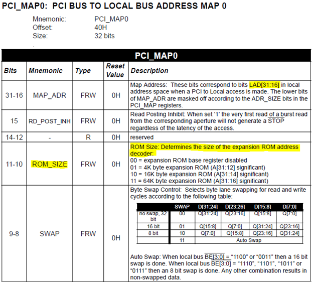
Figure 11 PCI_MAP0 register description. Courtesy: QuickLogic V363EPC datasheet
Figure 11 shows the ROM_SIZE bits in PCI_MAP0 register highlighted in yellow. The bits determine size of the PCI expansion ROM to be decoded by QuickLogic V363EPC. As you can see, the chip supports a PCI expansion ROM with size up to 64KB. Perhaps this size is not up to what a malicious PCI expansion ROM payload requires. However, a malicious PCI expansion ROM code can load additional code from other memory storage in the PCI add-in card when the ROM code executes. You must configure the ROM_SIZE bits default value to the correct value according to your hardware design. Entries in Figure 11 that have their "type" column marked as FRW means the default value of the bits are determined by the contents of the serial EEPROM if serial EEPROM support is activated via SDA and SCL "straps". Therefore, all you need to do is place the correct value in the serial EEPROM to configure their default values.
There is one more PCI configuration space register to take into account to implement BULLDOZER hardware, the Class Code register. The PCI Class Code register consists of three sub-parts: the base class, sub-class and interface. Figure 12 shows the class code selections for PCI Wireless Controller class of devices.

Figure 12 PCI Wireless Controller Class Code
As you see in Figure 12, we have to set the class code in our BULLDOZER chip design to base class 0Dh, sub-class 21h and interface 00h to make it masquerade as a PCI WLAN chipset that conforms to WLAN protocol revision B. Figure 7 shows the location of the Class Code register in the QuickLogic V363EPC chip. All you need to do is to store the correct class code in the serial EEPROM used to initialize contents of QuickLogic V363EPC PCI configuration space registers. This way our BULLDOZER design conforms to the PCI specification nicely.
At this point we can control the QuickLogic V363EPC PCI configuration space register's default values. We also have gained the required knowledge to map a PCI expansion ROM chip into the host x86/x64 CPU address space. The thing that's left to design is the way to store the BULLDOZER configuration.
Let's assume that we design the BULLDOZER configuration in an NVRAM chip. We can connect the NVRAM chip to SMT310Q PCI carrier board via the TIM interface, just like the PCI expansion ROM chip. The process to design the interconnection is similar to what we have done for the PCI expansion ROM chip. Except that we must expose the chip to code running on the host x86/x64 CPU via different aperture, for example by using PCI-to-Local Aperture 1.
Now, we know everything we need to implement a BULLDOZER hardware. There is one more thing left though, the "kill switch", i.e. the hardware to "destroy" evidence, just in case an operation involving BULLDOZER hardware gets botched.
Implementing "Kill Switch": Military-Grade Electronics Speculation
It's a standard procedure to have a kill switch in military electronics. A kill switch is a mechanism that enables you to destroy hardware or software remotely, that renders the hardware or software beyond repair. The destruction must be sufficient to prevent the software or hardware from being analyzed by anyone.
There are several reasons to have a kill switch. First, you don't want an adversary to find evidence to implicate you in the event that an operation fails. Second, you don't want your adversary to know your highly valued technology. There are other strategic reasons to have a kill switch, but those two suffice to conduct research into implementing a kill switch in BULLDOZER.
BULLLDOZER is a hardware that consists of several electronic chips "bounded" together via circuit board. Therefore, what we need to know is the technique to destroy the key chips in a circuit board at moment's notice. Surely, we turn to physics to solve this problem. From my experience as an overclocker in the past, I know very well that you can physically destroy a chip by inducing electromigration on it.
From Wikipedia: Electromigration is the transport of material caused by the gradual movement of the ions in a conductor due to the momentum transfer between conducting electrons and diffusing metal atoms.
Electromigration in simple terms means: the breakdown of metal interconnect inside a semiconductor chip due to migration of metal ions that construct the metal interconnect to an unwanted location. To put it simply, electromigration causes the metal interconnect inside the chip to be destroyed, akin to—but different from—corrosion in metal subjected to harsh environment. In many cases, electromigration can cause unwanted short circuits inside the chip. Figure 13 shows an electromigration illustration. As you can see, the copper ion (Cu+) moves in the opposite direction from the electrons. The copper ion is previously a part of the copper interconnect inside the semiconductor chip. The copper ion "migrates" to a different part of the chip due to electromigration.
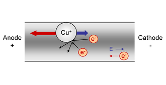
Figure 13 Electromigration. Courtesy: Wikipedia
There are many ways to induce electromigration on a semiconductor chip. However, I would focus only on one of them: overvoltage. You can induce electromigration by feeding excess voltage into a chip or into certain parts of a chip.
The problem now is designing a circuit to overvoltage only a certain part of a semiconductor chip. Let's assume that we don't want to overvoltage the entire chip, because we have previously assumed that BULLDOZER masquerades as a PCI WLAN chip. Therefore, you only want to destroy the part that implements the custom stealthy wireless communication protocol, not the part that implements the WLAN protocol. If the WLAN function was suddenly destroyed, you would raise suspicion on the target.
One of the way to create large voltage inside an electronic circuit is by using the so-called "charge pump". A charge pump is a DC to DC converter that uses capacitors as energy storage elements to create either a higher or lower voltage power source. As far as I know, it's quite trivial to implement a capacitor in a semiconductor chip. Therefore, using a charge pump to create our required overvoltage source should be achievable. Figure 14 shows one of the charge pump designs.

Figure 14 Dickson Charge Pump Design with MOSFETs. Courtesy: Wikipedia
Vin in Figure 14 is the source voltage that's going to be "multiplied". Vo in Figure 14 is the output voltage, i.e. a multiplication of the input voltage. As you can see, we can create voltage several times higher than the source voltage inside a semiconductor chip by using a charge pump. I have used a charge pump in one of my projects in the past. It's made of discrete electronics parts. The output voltage is usually not an exact multiple of the input voltage due to losses in the "multiplier" circuit. I suspect that a charge pump design implemented inside a semiconductor chip provides better "voltage multiplication" function compared to discrete ones.
At this point, we have all the things needed to create a kill switch. Your circuit design only needs to incorporate the charge pump into the design. You can use the control register in an FPGA to feed the logic on whether to activate the charge pump or not. You can devise certain byte patterns to turn on the charge pump to destroy your prized malicious logic parts in the PCI add-in card.
There are surely many ways to implement a kill switch. Using a charge pump is only one of the many. I present it here merely out of my "intuition" to solve the problem of creating a kill switch. The military surely has more tricks up their sleeve.
BULLDOZER Implementation Recap
We have gathered all the techniques needed to build a "BULLDOZER-equivalent" hardware in the previous sections. Surely, this is based on our earlier assumption that BULLDOZER masquerades as a PCI WLAN add-in card. Now, let's compose a recap, building on those newly acquired techniques and our assumptions in the beginning of this article. The recap is as follows:
- BULLDOZER is a malicious PCI add-in card that masquerades as a PCI WLAN card. It implements the correct PCI class code to masquerade as a PCI WLAN card.
- BULLDOZER implements a PCI expansion ROM because it's the delivery mechanism to "inject" GINSU malware code into the x86/x64 host system.
- BULLDOZER uses SDR to implement a stealthy wireless communication protocol to communicate with OMNIGAT.
- BULLDOZER was designed by using SDR FPGA prototyping tools before being fabricated as ASIC in the NSA's semiconductor fab. The NSA could use either Altera, Xilinx or internally-developed FPGA prototyping tools.
- BULLDOZER exposes the PCI expansion ROM chip via the XROMBAR in its PCI configuration space. The size of PCI expansion ROM chip exposed through XROMBAR is limited to 16MB, per the PCI specification. However, one can devise "custom" code to download additional content from the BULLDOZER PCI add-in card to system RAM as needed during the PCI expansion ROM execution. 16MB is already a large space for malicious firmware-level code though.
- It's not yet clear whether one desktop PC implanted with BULLDOZER is enough or more is required to make it work. However, the GINSU extended concept of operation implies that one BULLDOZER-implanted desktop PC is enough.
- A possibility not covered in this article is the NSA licensed design for the non-stealthy PCI WLAN controller chip part of BULLDOZER from commercial vendors such as Broadcom or Ralink. This could shorten the BULLDOZER design and implementation timeframe by quite a lot.
- Another possibility not covered here is BULLDOZER PCI chip being a multifunctioning PCI chip. The PCI bus protocol supports a single physical PCI controller chip that contains multiple functions. We don't delve into that possibility here though.
- As for the chip marking for the BULLDOZER PCI WLAN controller chip, it could easily carried out by the NSA fab. Well, with the right tool, anyone can even print the "I Love You" phrase as a legitimate-looking chip marking, like the one shown in Andrew "Bunnie" Huang blog: http://www.bunniestudios.com/blog/?p=3435.
That is all for our BULLDOZER implementation recap. It's quite a long journey, but we now have a clearer picture on BULLDOZER hardware implementation.

Cybersecurity interview guide
Closing Thoughts: BULLDOZER Evolution
Given that BULLDOZER was fielded almost six years ago, the present day BULLDOZER cranking out of the NSA's fab must have evolved. Perhaps into a PCI Express add-in card. It's quite trivial to migrate the BULLDOZER design explained in this article into PCI Express (PCIe) though. Therefore, the NSA shouldn't have any difficulty to carry out the protocol conversion. PCIe is compatible to PCI in the logical level of the protocol. Therefore, most of the non-physical design can be carried over from the PCI version of BULLDOZER design explained here. We should look into the "evolved" BULLDOZER in the future.

