System address map initialization in x86/x64 architecture part 2: PCI express-based systems
This article is the second part of a series that clarifies PCI expansion ROM address mapping to the system address map. The mapping was not sufficiently covered in my "Malicious PCI Expansion ROM"' article. You are assumed to have a working knowledge of PCI bus protocol and details of the x86/x64 boot process. If you don't, then please read the first part to get up to speed with the background knowledge required to understand this article.
The first part focuses on system address map initialization in a x86/x64 PCI-based system. This article focuses on more recent systems, i.e., x86/x64 PCI Express-based systems. From this point on, PCI Express is abbreviated as PCIe throughout this article, in accordance with official PCI Express specification.
We are going to look at system address map initialization in x86/x64 PCIe-based systems. Similar to the first part, the focus is on understanding the address mapping mechanism of the PCIe bus protocol. Knowledge of the address mapping is important to understand access to contents of the PCI expansion ROM in PCIe-based system.
PCIe is very different on the physical level from PCI. However, on the logical level PCIe is an extension of PCI. In fact, you can boot an OS only supporting the PCI bus on platforms using PCIe without a problem, as long as the OS support conforms to the PCI bus protocol specification. The fact that PCIe is an extension to PCI means that you should be familiar with the PCI bus protocol before you can understand PCIe. That's why you are strongly advised to read the first part before moving forward with this second part.
Conventions
This article uses these conventions:
- "Main memory" refers to RAM modules installed on the motherboard.
- "Memory controller" refers to that part of the chipset or the CPU that controls the RAM modules and controls access to the RAM modules.
- Flash memory refers to either the chip on the motherboard that stores the BIOS/UEFI or the chip on expansion card that stores the PCI expansion ROM contents.
- "Memory range" or "memory address range" means the range from the base/start address to the end address (base address + memory size) occupied by a device in the CPU memory space.
- "Memory space" means the set of memory addresses accessible by the CPU, i.e., the memory that is addressable from the CPU. Memory in this context could mean RAM, ROM, or other forms of memory that can be addressed by the CPU.
- "PCI expansion ROM" refers to the ROM chip on a PCI device or the contents of the chip, except when the context contains other specific explanation.
- The terms "hostbridge" and "northbridge" refer to the same logic components in this article. Both terms refer to the digital logic component that glues the CPU cores to the rest of the system, i.e., connecting the CPU cores to RAM modules, PCIe graphics, the "southbridge" chipset, etc.
- Intel 4th Generation Core Architecture CPUs are called "Haswell CPU" or simply "Haswell" in most of this article. Intel uses "Haswell" as the codename for this CPU generation.
- Hexadecimal values end with "h" as in 0B0Ah or starts with "0x" as in 0xB0A.
- Binary values end with "b" as in 1010b.
- The term "memory transactions routing" means memory transactions routing based on target address of the transaction, unless stated otherwise.
Another recurring word in this article is platform firmware. Platform firmware refers to code to initialize the platform upon reset, i.e., the BIOS or UEFI code residing in the flash ROM chip of the motherboard.
Preserving firmware code compatibility in modern-day x64 hardware
The x64 architecture is an extension of the x86 architecture. Therefore, x64 inherits most of the x86 architecture characteristics, including its very early boot characteristics and most of its system address map. There are two important aspects that x64 preserves from x86 with respect to firmware code execution:
- The CPU reset vector location. Even though x64 architecture is a 64-bit CPU architecture, the reset vector remains the same as in x86 (32-bit) architecture, i.e., at address 4GB-16 bytes (FFFF_FFF0h). This is meant to preserve compatibility with old add-on hardware migrated to x64 platforms and also compatibility with numerous low-level code depending on the reset vector.
- The "compatibility/legacy" memory ranges in the system address map. The "compatibility" memory ranges are used for legacy devices. For example, some ranges in the lowest 1MB memory area are mapped to legacy hardware or their hardware emulation equivalent. More important, part of the memory range is mapped to the bootblock part of the BIOS/UEFI flash ROM chip. The memory ranges for the BIOS/UEFI flash ROM didn't change because the CPU reset vector remains the same. Moreover, lots of firmware code depends on that address mapping as well. Breaking the compatibility from x86 would cause a lot of problems for the smooth migration to the x64 64-bit architecture, not counting on the business impact such a thing would cause. That's why preserving the compatibility between the two different architectures is important, down to the firmware and chip level.
Let's look at what is needed at the chip level to preserve the backward compatibility x86 architecture, now that you know the reason for preserving the compatibility. Figure 1 shows the logic components of the Haswell platform with relation to the UEFI/BIOS code fetch/read. As you can see, two blocks of logic, one in the CPU and one in the Platform Controller Hub (PCH), are provided to preserve the backward compatibility. They are the compatibility memory range logic in the CPU and the internal memory target decoder logic in the PCH. As for the Direct Media Interface (DMI) 2.0 controller logic, it's transparent with respect to software, including firmware code—it just acts as a very fast "pass-through" device; it doesn't alter any of the transactions initiated by the firmware code that pass through it.
Figure 1. BIOS/UEFI code read transaction in modern platform
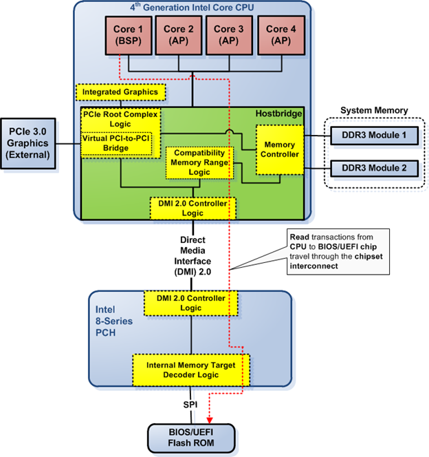
Figure 1 shows the CPU core fetching code from the BIOS/UEFI flash ROM connected to the PCH ("southbridge") via the serial peripheral interface (SPI)—see the dashed red line in Figure 1. This is what happened in the very early boot stage, when the CPU has just finished initializing itself and starts to fetch code located in the reset vector. The presence of "compatibility" logic in the platform, as shown in Figure 1, makes it possible to run DOS or 32-bit OS without any problems.
Figure 1 shows there are four CPU cores in the CPU. However, not all of them are the same; one of them is marked as boot strap processor (BSP), while the other three are marked as application processors (AP). When the system first boots or during a hardware reset, there is only one core that's active, the BSP. The APs are not active at that point. It's the job of the firmware (BIOS/UEFI) code that runs in the BSP to initialize and activate the APs during the system initialization phase.
Be aware though, that Figure 1 doesn't show all of the interconnections and hardware logic on both the CPU and the PCH, only those related to BIOS/UEFI code execution. The point is to highlight components that take part in very early BIOS/UEFI code execution after a system reset takes place.
As you can see in Figure 1, the transaction to reach the BIOS/UEFI flash ROM chip doesn't involve any PCIe logic or fabric; even if the hostbridge contains the PCIe root complex logic, the transaction doesn't go through it. Nonetheless, you still need to learn about PCIe bus protocol because the PCI expansion ROM that resides in a PCIe expansion card will use the PCIe fabric and logic. That's the reason PCIe-related sections are coming next in this article.
A deeper look into PCI-to-PCI bridge
PCIe hardware is logically represented as one PCI device or a collection of PCI devices. Some contain logical PCI-to-PCI bridge(s). The first part of this series doesn't delve much into PCI-to-PCI bridge. Therefore, we're going to take a much closer look into it here because it's used heavily as a logical PCIe device building block. For example, the root port ("outgoing" port from the root complex) is logically a PCI-to-PCI bridge and a PCIe switch logically looks like several connected PCI-to-PCI bridges.
We'll start dissecting PCI-to-PCI bridge by looking at its PCI configuration register header. PCI-to-PCI bridge must implement PCI configuration register type 1 header in its PCI configuration space register, unlike the header that must be implemented by non PCI-to-PCI bridge device—refer to the first part for PCI configuration register type 0 header. Figure 2 shows format of PCI-to-PCI bridge configuration space header, i.e. PCI configuration register type 1 header. This format is dictated by the PCI-to-PCI Bridge Architecture Specification v1.1 published by PCISIG.
Figure 2. PCI configuration register type 1 header (for PCI-to-PCI bridge)
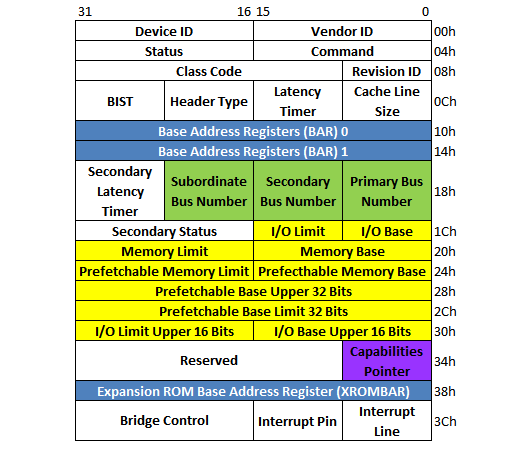
The numbers in the top of Figure 2 mark the bit position in the registers of the PCI configuration space header. The numbers to the right of Figure 2 mark the offset of the registers in the PCI configuration space header. Registers marked with yellow in Figure 2 determine the memory and IO range forwarded by the PCI-to-PCI bridge from its primary interface (the interface closer to the CPU) to its secondary interface (the interface farther away from the CPU). Registers marked with green in Figure 2 determine the PCI bus number of the bus in the PCI-to-PCI bridge primary interface (Primary Bus Number), the PCI bus number of the PCI bus in its secondary interface (Secondary Bus Number) and the highest PCI bus number downstream of the PCI-to-PCI bridge (Subordinate Bus Number).
NOTE:
Every PCIe device must set the Capabilities List bit in the Status register to 1 and every PCIe device must implement the Capabilities Pointer register (marked in purple in Figure 2). The reason is because PCIe is implemented as an extension to PCI protocol and the way to extend the configuration space of a PCIe device (compared to "ordinary" PCI device) is via the Capabilities Pointer register.
Figure 3 shows an illustration of PCI-to-PCI bridge primary and secondary interface in a hypothetical platform—the platform components' inner workings are the same with a real world system despite the platform is hypothetical; it's just simplified to make it easier to understand. PCI bus 1 connects to the PCI-to-PCI bridge primary interface and PCI bus 2 connects to the PCI-to-PCI bridge secondary interface in Figure 3.
Figure 3. PCI-to-PCI Bridge Interfaces
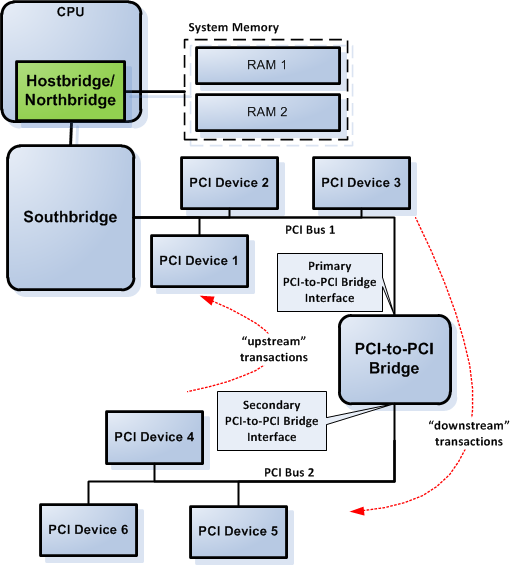
The PCI-to-PCI bridge forwards an IO transaction "downstream" (from the primary interface to the secondary interface) if the IO limit register contains a value greater than the IO base register value and the transaction address falls within the range covered by both registers. Likewise, the PCI-to-PCI bridge forwards a memory transaction "downstream" if the memory limit register contains a value greater than the memory base register value and the transaction address falls within the range covered by both registers.
There is a fundamental difference between the memory base/limit register and the prefetchable memory base/limit register. The memory base/limit registers are used for memory ranges occupied by devices that have a side effect on read transactions. The prefetchable memory base/limit registers are used only for devices that don't have side effects on read because, in this case, the PCI-to-PCI bridge can prefetch the data a on read transaction from the device without problems. Prefetching works because there is no side effect on the read transaction. Another difference is that the prefetchable memory base/limit registers are able to handle devices located above the 4GB limit because they can handle 64-bit address space.
There are no memory base/limit registers for devices mapped above 4GB because the PCI specification assumes all devices that require large address ranges behave like memory, i.e., their "memory" contents are prefetchable and don't have side effects on reads. Therefore, the PCI specification implies that devices with large address range consumption should implement prefetchable memory base/limit registers instead of memory base/limit registers and all devices with memory that have side effects on read should be mapped to address ranges below the 4GB limit by the platform firmware.
A fact sometimes overlooked when dealing with PCI-to-PCI bridge is that the bridge forwards memory transactions "upstream" (from the secondary interface to the primary interface<) — i.e., from PCI device to the direction of the CPU—if the transaction address range doesn't fall within the range covered by the memory base/limit or prefetchable memory base/limit registers. Perhaps, you're asking, why is this behavior needed? The answer is because we need direct memory access (DMA) to work for devices connected to the PCI-to-PCI bridge secondary interface. In DMA, the device "downstream" of the PCI-to-PCI bridge initiates the transaction (to read-from or write-to RAM) and the PCI-to-PCI bridge must ensure that the transaction is forwarded from the device in "upstream" direction toward the RAM.
Devices in DMA (in this case PCI devices) need to write data into the system memory—the so-called DMA write transaction. If you look at Figure 3, the DMA write transaction for devices connected to the PCI-to-PCI bridge secondary interface must go through the PCI-to-PCI bridge to reach the system memory; if the PCI-to-PCI bridge doesn't forward the write transaction "upstream," DMA cannot work because the contents from the device cannot be written to the system memory.
Now, let's have a look at an example of a memory transaction that's forwarded "downstream" by PCI-to-PCI bridge in Figure 3. Before we proceed to examine the example, we are going to make several assumptions:
- The system in Figure 3 has 8GB system memory. The first 3GB of the system memory is mapped to the lowest 3GB of the CPU memory address space; the rest is mapped to address range 4GB-to-9GB in the CPU memory address space—above the 4GB limit.
- The platform firmware has initialized all of the base address registers (BARs) of the PCI devices in the system; including the PCI-to-PCI bridge BARs. The platform firmware initialized the CPU memory range from 3GB to 4GB to be used by PCI devices; of course outside of the hardcoded range used by advanced programmable interrupt controller (APIC) logic, the platform firmware flash ROM chip and some other legacy system functions in the memory range close to the 4GB limit.
- Contents of the initialized PCI devices BARs and related registers are as follows:
- PCI device 1, only one BAR in use with 16 MB (non-prefetchable) memory space consumption starting at address E000_0000h (3.5GB). This BAR claims transactions to E000_0000h - E0FF_FFFFh non-prefetchable memory range.
- PCI device 2, only one BAR in use with 16 MB (non-prefetchable) memory space consumption starting at address E100_0000h (3.5GB + 16 MB). This BAR claims transactions to E100_0000h – E1FF_FFFFh non-prefetchable memory range.
- PCI device 3, only one BAR in use with 32 MB (prefetchable) memory space consumption starting at address E200_0000h (3.5GB + 32 MB). This BAR claims transactions to E200_0000h – E3FF_FFFFh prefetchable memory range.
- PCI device 4, only one BAR in use with 128 MB (prefetchable) memory space consumption starting at address C000_0000h (3GB). This BAR claims transactions to C000_0000h – C7FF_FFFFh prefetchable memory range.
- PCI device 5, only one BAR in use with 128 MB (prefetchable) memory space consumption starting at address C800_0000h (3GB + 128MB). This BAR claims transactions to C800_0000h – CFFF_FFFFh prefetchable memory range.
- PCI device 6, only one BAR in use with 256 MB (prefetchable) memory space consumption starting at address D000_0000h (3GB + 256MB). This BAR claims transactions to D000_0000h – DFFF_FFFFh prefetchable memory range.
- PCI-to-PCI bridge address and routing related configuration registers contents:
- Primary Bus Number Register: 1
- Secondary Bus Number Register: 2
- Subordinate Bus Number Register: 2 (Note: This is the same as secondary bus number because there is no other bus with higher number downstream of the PCI-to-PCI bridge)
- Memory Base: (Disabled)
- Memory Limit: (Disabled)
- Prefetchable Memory Base: C000_0000h (3GB)
- Prefetchable Memory Limit: DFFF_FFFFh (3.5GB - 1)
Now let's look at a sample read transaction with the PCI devices arrangement as in the assumptions above. Let's say the CPU needs to read data from PCI device at address D100_0000h (3GB + 16MB) to RAM. This is what happens:
- The CPU core issues a "read" transaction. This read transaction reaches the integrated hostbridge/northbridge.
- The northbridge forward the "read" transaction to the southbridge because it knows that the requested address resides in the southbridge.
- The southbridge forwards the "read" transaction to the PCI bus 1, which is connected directly to it.
- The PCI-to-PCI bridge claims the "read" transaction because it's within its assigned range. The PCI-to-PCI bridge claims the "read" transaction and responds to it because the requested address is within the range of its prefetchable memory range (between the value of the prefetchable memory base and prefetchable memory limit).
- The PCI-to-PCI bridge forwards the "read" transaction to its secondary bus, PCI bus 2.
- PCI device 6 claims the "read" transaction in PCI bus 2 because it falls within the range of its BAR.
- PCI device 6 returns the data at the target address (D100_0000h) via PCI bus 2.
- The PCI-to-PCI bridge forwards the data to the southbridge via PCI bus 1.
- The southbridge forwards the data to the CPU.
- The northbridge in the CPU then places the data in RAM and the read transaction completes.
From the sample above, you can see that the PCI-to-PCI bridge forwards read/write transaction from its primary interface to its secondary interface if the requested address falls within its range. If the read/write transaction doesn't fall within its configured range, the PCI-to-PCI bridge would not forward the transaction from its primary interface to its secondary interface.
A seldom known fact about PCI-to-PCI bridge is the presence of a subtractive decode PCI-to-PCI bridge. The "decoding" method explained in the example above—to claim the "read" transaction—is known as positive decode, i.e., the device claims the transaction if it's within its assigned range (in one of its BAR). The reverse of positive decode is known as subtractive decode. In subtractive decode the device—with subtractive decode support—claims the transaction if there is no other device on the bus that claims the transaction, irrespective of whether the transaction is within the device range or not. There could only be one subtractive decode device in one PCI bus tree. There is a certain class of PCI-to-PCI bridge device that supports subtractive decode. It was used to support address decoding of legacy devices—such as a BIOS chip—in older chipsets. However, this technique is largely abandoned in modern-day chipsets because there is already legacy-support logic in the chipset and the CPU.
PCIe device types
You have learned all the required prerequisites to understand PCIe protocol in the previous section. Now let's start by looking into PCIe device types based on their role in a PCIe device tree topology. This is important to understand because you need a fundamental understanding of PCIe device types to understand PCIe devices initialization. PCIe devices are categorized as follows:
- PCIe root complex. The root complex is similar to northbridge in PCI-based system. It acts as the "glue" logic to connect the PCIe device tree to main memory (RAM), and the CPU. In many cases, the root complex also provides high speed PCIe connection to the GPU. The root complex can be implemented as part of the northbridge in systems that employ two physical chips for the chipset logic. However, nowadays the root complex is always integrated into the CPU chip, as you can see in Figure 1. Figure 1 shows the PCIe root complex as part of the hostbridge that's integrated into the CPU. The root complex connects to the PCIe device tree through a logical port known as root port. It is a logical port because the root port can be implemented physically in a chip outside the chip containing the root complex. For example, the root complex can reside in the CPU, but the root port is located in the chipset. The Haswell CPU and Intel 8-series PCH implements this root port arrangement. Note that the root complex can have more than one root port.
- PCIe switch. A PCIe switch is a device that connects two or more PCIe links. A switch contains several connected virtual PCI-to-PCI bridges internally. That is the reason why you should have a deep understanding of PCI-to-PCI bridge in order to understand PCIe device tree topology. Anyway, the root complex can contain a switch, in which case the root complex will have several root ports.
- PCIe endpoint device. This is the PCIe device type that most people know as a PCIe device. A PCIe endpoint device is a PCIe device that terminates a PCIe link; it only has one connection to the PCIe tree topology—it can have connection to another kind of bus, though. For example, a PCIe network card in most cases is an endpoint device, just as PCIe storage controller, etc. PCIe endpoint device can also act as a bridge to legacy/compatibility bus, such as a PCIe-to-PCI bridge, or a bridge to a low pin count (LPC) bus, etc.
Perhaps the explanation of a PCIe switch and endpoint device is still vague. Figure 4 shows an example of a PCIe switch and endpoint devices in a PCIe device tree topology. Figure 4 shows that the PCIe switch is composed of three connected "virtual" (logical) PCI-to-PCI bridges. The switch has one inbound port (called an ingress port in PCIe) and two outbound ports (called egress ports in PCIe). There are two endpoint devices connected to the switch, an add-in network and an add-in SCSI controller. Each of the endpoint devices connect to the switch via the switch's virtual PCI-to-PCI bridges.
Figure 4 shows the physical location of the root ports of the PCIe root complex. One is directly connected to the PCIe root complex and the other is not directly connected to the PCIe root complex—i.e.. connected via the chipset interconnect. In the latter case, the chipset interconnect is said to be transparent with respect to PCIe device tree topology. Figure 4 shows the external PCIe graphics links to the root port that's located in the PCIe root complex while the PCIe switch links to the root port via the chipset interconnect. There is no difference between them from a PCIe logic point of view.
Figure 4. PCIe switch and endpoint devices
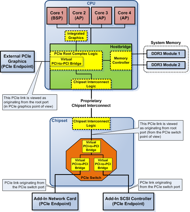
Figure 4 shows the interconnection between PCIe devices. This interconnection is called a link in PCIe bus protocol. The link is a logical interconnection that connects two PCIe ports on two different PCIe devices. Each link consists of one or more lanes. Each lane consists of a pair of physical interconnects, one in the outgoing direction from the PCIe device and one in the incoming direction to the PCIe device. The physical interconnect uses differential signaling to transmit the PCIe packets in either direction.
At this point, PCIe device basics should be clear to you. In the next section I'll go through the details of communication between PCIe devices.
PCIe packets and device layering
One of the major differences between PCIe and PCI bus protocol is the implementation of a higher level of abstraction in PCIe. Each transaction in PCIe is wrapped into a PCIe packet before it's transmitted to another PCIe device. Therefore, PCIe is a packet-based protocol for chip-to-chip communication. This fact has the consequence that PCIe has the capability to implement quality of service (QoS) via packet prioritization. However, I'm not going to explain about the QoS in PCIe, you just need to know QoS exists in PCIe.
Now let's get to the packet details. PCIe protocol employs the same philosophy as TCP/IP in that it uses several communication layers, with each layer appending "header" to the content of the packet to provide routing, error correction and other housekeeping. Figure 5 shows how PCIe implements this philosophy.
Figure 5. PCIe packet-based communication
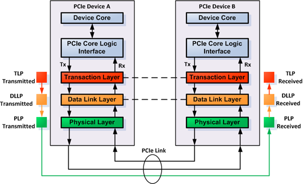
There are three types of packets in PCIe protocol (as seen from the highest level of abstraction down to lowest level packet sent over the PCIe link):
- Transaction layer packet (TLP)—The transaction layer in the PCIe device constructs this packet, as seen in Figure 5. the TLP consists of a TLP header and the data content being transmitted. The source of the data content is the PCIe device core and the PCIe core logic interface in the device. The TLP header contains CRC, among other data. TLP can travel through the PCIe device tree, passing through more than one PCIe devices between the source and the destination device. This looks like the packet "tunnels" through the PCIe device in between the source and the destination. But in reality the packet is just routed through the PCIe device tree. The PCIe device in between the source and the destination must be a PCIe switch because only a switch can forward/route packets from its ingress port to its egress port.
- Data link layer packet (DLLP)—The data link layer in the PCIe device constructs this packet, as seen in Figure 5. DLLP wraps the TLP in yet another header. DLLP provides another CRC for the packet in the DLLP header. DLLP can only travel between PCIe devices directly connected to each other through a PCIe link. Therefore, the purpose of the CRC is different from that provided by the TLP because DLLP CRC is used to make sure that the neighboring PCIe device receives the packet correctly. There are also some specific DLLPs which don't contain any TLP packet inside of it, such as DLLP for link power management, flow control, etc.
- Physical layer packet (PLP)—The physical layer in the PCIe device constructs this packet, as seen in Figure 5. PLP wraps the DLLP into one or several PLPs, depending on the size of the DLLP; if the size of the DLLP cannot fit into a single PLP, the PLP logic divides the DLLP into several "frames" of PLPs. The PLPs are transmitted in the link between two connected PCIe devices. There are also some specific PLPs that don't contain any DLLP packet, such as PLP for link training, clock tolerance compensation, etc.
The explanation about PCIe packet types above implies that a PCIe device must have three device layers, one for each type of packet. In practice, that's not always the case. As long as the PCIe device can create PCIe packets that conform to the specification, it's fine.
PCIe address spaces
You know from the previous section that PCIe is a packet-based chip-to-chip communication protocol. This means that the protocol requires some means to route the DLLP or TLP between chips. DLLP can only reach directly linked PCIe chips. Therefore, we are more interested in TLP routing because in several cases the target of a read/write transaction lies several chips away from the source of the read/write transaction. There are several mechanisms to route the TLP. Here, we are going to look into one of them, namely, the TLP routing based on address, also known as address routing.
There are four address spaces in PCIe. In contrast, PCI only have three address spaces. PCIe address spaces are as follows:
- PCIe configuration space—This address space is used to access the PCI-compatible configuration registers in PCIe devices and also the PCIe enhanced configuration registers. Part of this address space that resides in the CPU IO space is provided for backward compatibility reasons—i.e., compatibility with PCI bus protocol. The rest of the PCIe configuration space resides in the CPU memory space. The access mechanism for the first 256 registers is the same as in PCI for x64 architecture, i.e., using IO port 0xCF8-0xCFB for address and 0xCFC-0xCFF for data. As in PCI devices, there are 256 eight-bit configuration space registers that are mapped to this IO address space in PCIe. The first 256 byte configuration registers are immediately available at the very early boot stage via the CPU IO space (because the mapping doesn't require firmware initialization), while the rest are available only after the platform firmware finishes initializing CPU memory space used for PCIe configuration space. PCIe supports a larger number of configuration space registers than PCI. Each PCIe device has 4KB configuration space registers. The first 256 bytes of those registers are mapped to both the "legacy" PCI configuration space and to PCIe configuration space in the CPU memory space. The entire 4KB PCIe configuration space registers can be accessed via PCIe enhanced configuration mechanism. PCIe enhanced configuration mechanism uses the CPU memory space instead of the CPU IO space (PCI configuration mechanism uses the CPU IO space in x86/x64 architecture).
- PCIe memory space—This address space lies in the CPU memory address space, just as in PCI. However, PCIe supports 64-bit addressing by default. Part of the PCIe configuration register is located in the PCIe memory space. However, what is meant by PCIe memory space in this context is the CPU memory space consumed by PCIe devices for non-configuration purposes. For example, the CPU memory space used to store PCIe device data, such as for local RAM in PCIe network controller card or PCIe graphics card local RAM used for graphics buffer.
- PCIe IO space—This is the same as the IO space in PCI bus protocol. It exists only for PCI backward compatibility reason.
- PCIe message space—This is a new address space not previously implemented in PCI. This address space exists to eliminate the need for physical sideband signals. Therefore, everything that used to be implemented physically in previous bus protocols, such as the interrupt sideband signal, is now implemented as messages in the PCIe device tree. We are not going to look deeper into this address space. It's enough to know its purpose.
This article only deals with two address spaces of the four PCIe address spaces explained above, PCIe configuration space and PCIe memory space. We are going to look into the PCIe configuration space in the PCIe configuration mechanism section later. In this section, we're going to look into the PCIe memory space in detail.
For the sample, we're going to proceed to scrutinize a PCIe memory read transaction that goes through the PCIe fabric (device tree), a read transaction routed via address-routing. We're going to look at a quite complicated PCIe platform that contains a PCIe switch. This kind of configuration usually doesn't exist on a desktop-class PCIe platform, only on a server-class PCIe platform. The complexity of the sample would make it a lot easier for the reader to deal with desktop-class hardware in a real-world scenario because the latter is simpler compared to server-class platform.
Figure 6 shows the sample memory read transaction with targets address at C000_0000h (3GB). The memory read transaction originated in the CPU core 1, and the target is the contents of the PCIe Infiniband "network" controller "local" memory because that address is mapped to the latter device's memory. The transaction is routed through the PCIe fabric. The double arrow in the read transaction path in Figure 6—marked as a dashed purple line—indicates that the path taken to get to the PCIe device memory contents is identical to the path taken by the requested data back to CPU core 1.
Address-routing in the PCIe fabric can only happen after all the address-related registers in all PCIe devices in the fabric are initialized. We assume that the platform firmware initializes the platform in Figure 6 as follows:
- The system has 8GB RAM; 3GB mapped to the 0-to-3GB memory range and the rest mapped to the 4GB-to-8GB memory range. The mapping is controlled by the respective mapping registers in the hostbridge.
- The PCIe Infiniband network controller has 32MB of local memory, mapped to addresses C000_0000h to C1FF_FFFFh (3GB to 3GB+32MB-1).
- The PCIe SCSI controller card has 32MB of local memory, mapped to addresses C200_0000h to C3FF_FFFFh (3GB+32MB to 3GB+64MB-1).
- Virtual PCI-to-PCI bridge 1, 2, and 3 don't claim memory or an IO range for themselves, i.e., BAR 0 and BAR 1 of each of these devices are initialized to values that don't claim any memory ranges.
- Virtual PCI-to-PCI bridge 1 claims memory range C000_0000h to C3FF_FFFFh (3GB to 3GB+64MB-1) as prefetchable memory.
- Virtual PCI-to-PCI bridge 2 claims memory range C000_0000h to C1FF_FFFFh (3GB to 3GB+32MB-1) as prefetchable memory.
- Virtual PCI-to-PCI bridge 3 claims memory range C200_0000h to C3FF_FFFFh (3GB+32MB to 3GB+64MB-1) as prefetchable memory.
With all the memory-related stuff initialized, we can proceed to see how the read transaction travels through the PCIe fabric.
Figure 6. PCIe memory read transaction sample going through the PCIe fabric via address routing
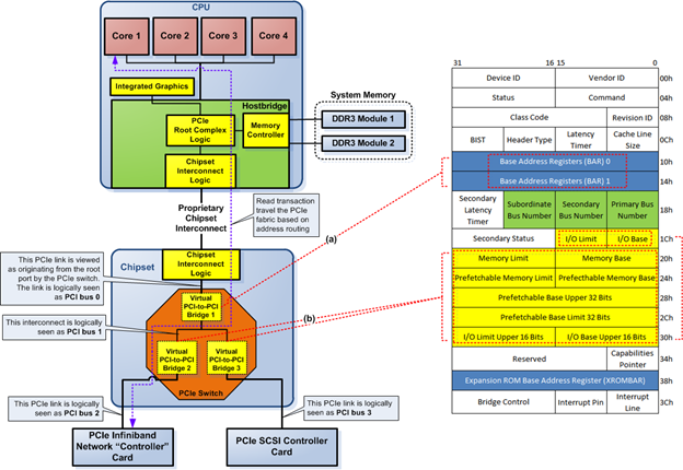
Now let's look at the steps taken by the read transaction shown in Figure 6:
- The memory read transaction with target address at C000_0000h originated in the CPU's core 1.
- The memory read transaction reaches the hostbridge. The hostbridge mapping register directs the transaction to the PCIe root complex logic because the address maps to the memory range claimed by PCIe.
- The PCIe root complex logic in the hostbridge recognizes the memory read transaction as targeting the PCIe fabric—due to the hostbridge mapping registers setting—and converts the memory read transaction into a PCIe read TLP.
- The TLP is placed in "logical" PCI bus 0. PCI bus 0 originates in the PCIe root complex logic and ends in virtual PCI-to-PCI bridge 1 in the PCIe switch inside the chipset. Note that the chipset interconnect logic is transparent with respect to PCI and PCIe protocol.
- Virtual PCI-to-PCI bridge 1 checks the target address of the TLP. In the beginning, virtual PCI-to-PCI bridge 1 checks whether the TLP target address is within virtual PCI-to-PCI bridge 1 itself by comparing the target address with the value of its BAR 0 and BAR 1 registers. However, virtual PCI-to-PCI bridge 1 BAR 0 and BAR 1 don't claim any memory read/write transaction as per the platform firmware initialization value. Then it checks whether the target address of the TLP is within the range of one of its memory base/limit or prefetchable memory base/limit registers. Figure 6 shows both of these steps in point (a) and (b). Virtual PCI-to-PCI bridge 1 found that the target address of the TLP is within the range of the range of its prefetchable memory range. Therefore, the Virtual PCI-to-PCI bridge 1 accepts the TLP in PCI bus 0 and routes the TLP to PCI bus 1.
- Virtual PCI-to-PCI bridge 2 and virtual PCI-to-PCI bridge 3 do a similar thing to the TLP in PCI bus 1 as virtual PCI-to-PCI bridge 1 did on PCI bus 0, i.e., check their own BARs and their memory base/limit and prefetchable memory base/limit. Virtual PCI-to-PCI bridge 2 found that the TLP target address is in its secondary interface. Therefore, virtual PCI-to-PCI bridge 2 accepts the TLP in PCI bus 1 and routes the TLP to PCI bus 2.
- The PCIe Infiniband network controller in PCI bus 2 checks the target address of the TLP routed by virtual PCI-to-PCI bridge 2 and accepts the TLP because the target address is within the range of one of its BARs.
- The PCIe Infiniband network controller returns contents of the target address to the CPU via the PCIe fabric. Note: we are not going to scrutinize this process in detail because we have learned the details of the TLP address-based routing from the CPU to the PCIe Infiniband network controller.
At this point, PCIe address spaces and PCIe address routing should be clear. The next section focuses on PCIe configuration space and the mechanism for routing PCIe configuration transactions to their targets.
PCIe configuration mechanisms
You need to know PCIe configuration mechanisms because they are the methods used to initialize all of the PCIe devices in a platform that implements PCIe. There are two types of configuration mechanisms in PCIe. as follows:
- The PCI-compatible configuration mechanism—This configuration mechanism is identical to the PCI configuration mechanism. On an x86/x64 platform, this configuration mechanism uses IO port CF8h-CFBh as the address port, and IO port CFCh-CFFh as the data port to read/write values from/into the PCI configuration register of the PCIe device. This configuration mechanism can access 256-bytes configuration registers per device—refer to the PCI configuration register section in the first part of this series (at /system-address-map-initialization-in-x86x64-architecture-part-1-pci-based-systems/) for details on PCI configuration mechanisms. PCIe supports 4KB of configuration registers per device, in contrast to "only" 256 bytes supported by PCI. The rest of the configuration registers can be accessed via the second PCIe configuration mechanism, the PCIe enhanced configuration mechanism.
- The PCIe enhanced configuration mechanism—In this configuration mechanism, the entire PCIe configuration registers all of the PCIe devices that are mapped to the CPU memory space, including the first 256-bytes PCI-compatible configuration registers, which are mapped to both the CPU IO space and the CPU memory space—see point 1 above. The CPU memory range occupied by the PCIe configuration registers must be aligned to the 256MB boundary. The size of the memory range is 256MB. The calculation to arrive in this memory range size is simple: each PCIe device has 4KB configuration registers, PCIe supports the same number of buses as PCI, i.e. 256 buses, 32 devices per bus, and 8 functions per device. Therefore, the total size of the required memory range is: 256 x 32 x 8 x 4KB; which is equal to 256MB.
One of the implications of the PCIe configuration mechanism is that the first 256-bytes of each of the PCIe device configuration registers are mapped into two different spaces, the CPU IO space—through the PCI-compatible configuration mechanism—and the CPU memory space—through the PCIe enhanced configuration mechanism. If you are still confused about this explanation, take a look at Figure 7. Figure 7 shows mapping of the PCIe device configuration space registers of one PCIe device into the CPU IO space and CPU memory space.
Figure 7. PCIe device configuration space register mapping as seen from the CPU
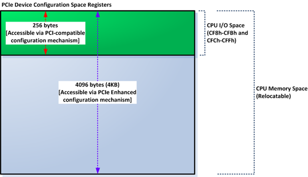
You might be asking why PCIe systems still need to implement the PCI configuration mechanism. The first reason is to provide backward-compatibility to operating systems that existed prior to the PCIe being adopted and the second reason is to provide a way to initialize the PCIe enhanced configuration mechanism. On an x64 platform, the CPU memory range consumed by the PCIe enhanced configuration mechanism is not hardcoded to a certain CPU memory range, it's relocatable in the 64-bit CPU memory space. The platform firmware must initialize certain register in the PCIe root complex logic to map the PCIe devices' configuration registers to certain address in the 64-bit CPU memory space. The start address to map the PCIe configuration registers must be aligned to 256MB boundary. On the other hand, location of the PCI configuration registers in the CPU IO space is hardcoded in x86 and x64; this provides a way to initialize the register that controls the mapping of all of the PCIe configuration registers—in the PCIe root complex—via PCI-compatible configuration mechanism because PCI-compatible configuration mechanism is available at all times, including very early at system boot.
A PCIe enhanced configuration mechanism has an implication that reading or writing the PCIe configuration registers of a PCIe device requires a memory read or write. This is a contrast to the PCI configuration mechanism, where the code to do the same thing requires an IO read or IO write. This approach was a trend in the hardware world in the late 90's—i.e., moving all hardware-related registers to CPU memory space to simplify hardware and system software design. It was not adopted just by the PCIe bus protocol but also by other bus protocols in CPU architectures other than x64.
Figure 8. PCIe enhanced configuration mechanism address bits mapping to CPU memory space

Figure 8 shows mapping of the PCIe enhanced configuration space into the 64-bit CPU memory space. This is the breakdown of the 64-bit PCIe enhanced configuration space register address:
- Address bits 28-63 are upper bits of the 256MB-aligned base address of the 256MB memory-mapped IO address range allocated for the enhanced configuration mechanism. The manner in which the base address is allocated is implementation-specific. Platform firmware supplies the base address to the OS. Mostly, the base address is controlled by a programmable register that resides in the chipset or is integrated into the CPU.
- Address bits 20-27 select the target bus (1-of-256).
- Address bits 15-19 select the target device (1-of-32) on the bus.
- Address bits 12-14 select the target function (1-of-8) within the device.
- Address bits 2-11 select the target double-word (a.k.a. dword); 1-of-1024 within the selected function's configuration space.
- Address bits 0-1 define the start byte location within the selected dword.
As in PCI configuration register address accesses, reading or writing to PCIe enhanced configuration registers must be aligned into a dword (32-bit) boundary. This is because the CPU and the chipset in the path to the PCIe enhanced configuration register only guarantee the delivery of configuration transactions if they are aligned to a 32-bit boundary.
In x64 architecture, a special register in the CPU—part of the PCIe root complex logic—controls the 36-bit PCIe enhanced configuration space base address. This base address register must be initialized by the platform firmware on boot. The register initialization is carried out through a PCI-compatible configuration mechanism because, at very early boot, the register contains a default value that is not usable to address the registers in the PCIe enhanced configuration space. We'll have a look deeper into the implementation of this base address when we dissect the PCIe-based system address map later.
Now, let's look at a simple example of PCIe enhanced configuration register mapping into the CPU address space. Let's make these assumptions:
- The base address of the PCIe enhanced configuration address space is set to C400_0000h (3GB+64MB) in the PCIe root complex register.
- The target PCIe device resides in bus number one (1).
- The target PCIe device is device number zero (0) in the corresponding bus.
- The target PCIe function is function number zero (0).
- The target register resides at offset 256 (100h) in the PCIe device configuration space.
- Size of the target register is 32 bits (1 dword).
With the assumptions above, we found out that the target PCIe enhanced configuration register resides at address C410_0100h. The higher 32-bit value of the PCIe enhanced configuration register address is practically 0; the target address only uses the lower 32-bit of the CPU memory address space. If the target address that corresponds to the target PCIe configuration register is still confusing, break it down according to the mapping shown in Figure 8. It should be clear after that.
PCIe capabilities register set
There are several fundamental differences between PCIe and "legacy" PCI devices. We are going to look into one of those differences before we move on to PCIe BAR initialization because they affect PCIe BAR implementation, the PCIe capabilities register set. All PCIe devices must implement the PCIe capabilities register set in the first 256 bytes of its configuration space registers. In contrast, a "legacy" PCI device is not required to implement any capabilities register set. In "legacy" PCI devices, implementing a capabilities pointer is optional, not mandatory. Figure 9 shows implementation of the PCIe capabilities register set in a PCIe device configuration space register.
Figure 9. PCIe device capabilities register set
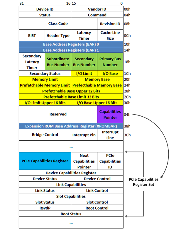
Figure 9 shows a capabilities pointer register—highlighted in purple—in PCIe device configuration space pointing to the PCIe capabilities register set. In practice, the capabilities pointer register points to the start of PCIe capabilities register set by using an 8-bit offset (in bytes) of the start of PCIe capabilities register set. The offset is calculated from start of the PCIe device configuration space. This 8-bit offset is stored in the capabilities pointer register. The position of the PCIe capabilities register set is device-specific. However, the PCIe capabilities register set is guaranteed to be placed in the first 256 bytes of the PCIe device configuration space and located after the mandatory PCI header. Both a type 0 or type 1 header must implement the PCIe capabilities register set in a PCIe device configuration space.
Now, let's look more closely at part of the PCIe capabilities register set. Figure 9 shows the third register in the capabilities register set is the PCIe capabilities register. Figure 10 shows format of this register's contents.
Figure 10. PCIe capabilities register format
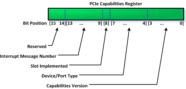
Device/port type bits (bits 4-7) in the PCIe capabilities register are the ones that affect the PCIe device mapping to the system address map. Device/port type bits determine whether the PCIe device is a native PCIe endpoint function or a legacy PCIe endpoint function. Differences between the two types of PCIe device are:
- The value of device/port type bits in a native PCIe endpoint function is 0000b. Native PCIe endpoint function devices must map all of the device components, such as its registers and local memory, to the CPU memory space at runtime—from inside a running OS. The only time the device is permitted to use the CPU IO space is during early boot time, before the platform firmware finishes initializing the system.
- Value of device/port type bits in a legacy PCIe endpoint function is 0001b. Legacy PCIe endpoint function devices are permitted to use the CPU IO space even at runtime. The PCIe specification assumes that legacy PCIe endpoint function devices act as front-end to legacy bus, such as PCI or PCI-X.
Now, it's clear that the contents of the PCIe capabilities register determine whether the PCIe device will map its BARs to the CPU memory space or to the CPU IO space at runtime. There are special cases though, especially when dealing with legacy IO devices. For example, legacy PC-compatible devices such as VGA and IDE controllers frequently expect to be located within fixed legacy IO ranges. Such functions do not implement base address registers. Instead, the configuration software identifies them as legacy functions via their respective class codes—offset 09h in the PCIe configuration space—and then enables their IO decoder(s) by setting the IO space bit in its command register to one.
PCIe base address register initialization
PCIe devices use BAR just like PCI devices. Therefore, a PCIe device's BAR must be initialized before the device can be used. PCI BAR initialization is the job of the platform firmware. The PCI specification provides implementation notes on PCI BAR initialization. PCIe continues to support this BAR initialization method.
I'm not going to repeat the explanation PCI BAR initialization here; I'm only going to highlight the differences between PCIe BAR initialization and PCI BAR initialization in this section. Please refer to the first part of the series for the basics of PCI BAR formats and PCI BAR initialization (at /system-address-map-initialization-in-x86x64-architecture-part-1-pci-based-systems/).
PCIe BAR formats
There are two types of BAR: The first is a BAR that maps to the CPU IO space—an IO BAR—and the second one is a BAR that maps to the CPU memory space—a memory BAR. A PCIe IO BAR is exactly the same as a PCI IO BAR. However, the PCIe specification recommends abandoning using the IO BAR for new PCIe devices. These new devices should use the memory BAR instead.
Figure 11. PCI/PCIe memory BAR format
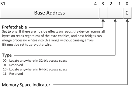
Figure 11 shows the memory BAR format. Figure 11 shows that the lowest bit is hardcoded to 0 in the BAR that map to CPU memory space. It also shows that bit 1 and bit 2 determine whether the BAR is a 32-bit BAR or 64-bit BAR.
Figure 11 shows that bit 3 controls the prefetching in the BAR that map to CPU memory space. Prefetching in this context means that the CPU fetches the contents of memory addressed by the BAR before a request to that specific memory address is made, i.e., the "fetching" happens in advance, hence "pre"-fetching. This feature is used to improve the overall PCI/PCIe device memory read speed.
The main difference between a PCI and PCIe memory BAR is that all memory BAR registers in PCIe endpoint functions with the prefetchable bit set to 1 must be implemented as 64-bit memory BARs. Memory BARs that do not have the prefetchable bit set to 1 may be implemented as 32-bit BARs. The minimum memory range requested by a memory BAR is 128 bytes.
Another difference between PCIe and PCI is the notion of a dual address cycle (DAC). PCIe is a serial bus protocol and doesn't implement DAC. PCIe was designed with native 64-bit addressing in mind. Therefore, support for memory transactions targeting 64-bit addresses is native in PCIe. There is no performance penalty for carrying out memory transactions targeting 64-bit addresses.
PCIe BAR sizing
The algorithm for PCIe BAR sizing is the same as the algorithm for PCI device BAR sizing explained in the first article. The difference lies only in prefetchable memory BAR, because a prefetchable memory BAR in PCIe must be 64 bits wide, the BAR sizing algorithm must use two consecutive 32-bit BARs instead of one 32-bit BAR during BAR sizing.
Dissecting PCIe-based system address map
In this section we look at an implementation sample of the system address map in x86/x64 before proceeding to the system address map initialization in more detail. The implementation sample is based on Haswell—with integrated northbridge/hostbridge—and the Intel 8-series PCH platform. This platform implements the PCIe bus and it's an up-to-date platform. Therefore, it's a perfect example to learn real-world PCIe implementation.
Intel 8-series PCH can be viewed as southbridge in the classic system layout; however, both are not the same logic because there are some functions in the PCH that absent in the "classic" southbridge. You can download the CPU datasheet from http://www.intel.com/content/www/us/en/processors/core/CoreTechnicalResources.html and PCH datasheet from http://www.intel.com/content/www/xr/en/chipsets/8-series-chipset-pch-datasheet.html.
PCIe differs from PCI in that PCIe moves everything to CPU memory space, including its configuration space, as you can see from the PCIe configuration mechanisms section. The presence of part of PCIe configuration registers in the CPU IO space is only for backward compatibility reasons. This fact means the CPU memory space in a PCIe-based system is a bit more fragmented compared to PCI-based systems. However, this approach pays back in terms of less complication in CPU design and quicker access to all of the memory ranges mapped to the CPU memory space, including PCIe configuration registers, because access to CPU memory space is quicker than access to IO space by default.
Haswell CPU and Intel 8-series chipset platform
Figure 12 shows a block diagram of systems with Haswell CPU and 8-series chipset combination. Figure 12 shows the entire connection from the chipset to other components in the system, including those that might not exist in all chipset stock keeping units (SKUs).
Figure 12. Intel Haswell CPU with 8-series chipset block diagram
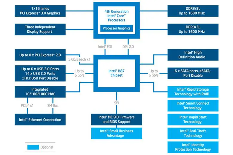
Not all of the system interconnects in Figure 12 affect the system address map. We are going to focus only on interconnects and control registers that affect the system address map in this article. The interconnects of interest in Figure 12 are the DMI 2.0 interconnect, the interconnect from CPU to PCIe graphics, the SPI interconnect from the Intel H87 chipset to the platform firmware, the interconnect from the Intel H87 chipset to PCIe devices, and the interconnect from the CPU to DDR3 DRAM modules. We will get into the details of memory transactions routing to these interconnects in the next section (Haswell Memory Transactions Routing).
Haswell memory transactions routing
Address-based memory transactions routing in Haswell CPU determines the system memory map. There are several control registers in the hostbridge part of the CPU that control memory transaction routing in this platform. Before we get into the registers details, we'll have a look at the high-level view of the memory transaction routing in the northbridge. Figure 13 shows the logic components in the northbridge that takes care of memory transaction routing. You won't see these logic blocks depicted in any of the publicly available datasheet from Intel. I draw them in Figure 13 based on details provided in the datasheet. The logic blocks are "abstractions" to make the memory transaction routing understandable.
Figure 13. Memory transactions routing in Haswell Northbridge/Hostbridge
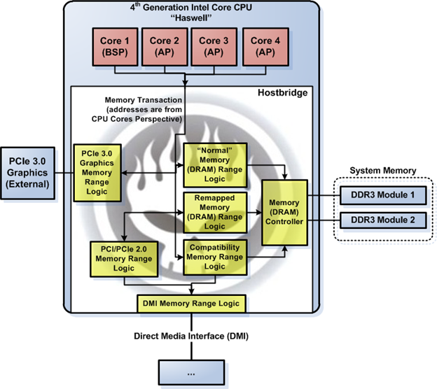
Memory transactions in Figure 13 originate in the CPU and target DRAM, DMI, or the external PCIe graphics. We are not going to delve into direct memory access (DMA) in this article because DMA can originate in the PCIe graphics or the DMI. This means that the DMA adds unnecessary complications to understanding memory transaction routing in the hostbridge.
Figure 13 shows five different memory transaction routing logic blocks that connect directly to Haswell CPU cores. The memory transaction routing logic blocks are as follows:
- "Normal" DRAM range logic—This logic block routes memory transactions (read/write) targeting the range covered by DRAM, which requires no remapping, i.e., the target address of the transaction doesn't need any translation before entering the memory/DRAM controller. The control registers that control this memory range are top of low usable DRAM (TOLUD) register and remap base register. Both registers are in the hostbridge. TOLUD controls CPU memory range occupied by the DRAM below 4GB. Remap base is only in use if the system DRAM size is equal to or larger than 4GB; in this case remap base marks the end of the "normal" CPU DRAM range above 4GB.
- Remapped DRAM range logic—This logic block routes memory transactions (read/write) targeting range covered by DRAM that requires remapping, i.e., the target address of the transaction need to be translated before entering the memory/DRAM controller. There are two control registers that control the remapped memory range, the remap base and remap limit registers. The registers are in the hostbridge.
- Compatibility memory range logic—This logic block routes memory transactions (read/write) targeting range covered by the compatibility memory range. This memory range comprises the range between A_0000h to F_FFFFh and the ISA hole from F0_0000h to F_FFFFh (15MB to 16MB). This memory range is further divided into three sub-ranges:
- Legacy VGA memory range lies between A_0000h and B_FFFFh—VGA memory map mode control register controls mapping of compatibility memory range from A_0000h to B_FFFFh. This range may be mapped to PCIe, DMI or Internal Graphics Device (IGD), depending on the VGA memory map mode control register value. Therefore, a memory transaction targeting memory ranges between A_0000h and B_FFFFh will be routed to either PCIe or DMI or IGD.
- Non-VGA compatibility and non-"ISA Hole" memory range, which consists of memory range from C_0000h to F_FFFFh—All memory transactions targeting this compatibility memory range are routed either to the memory/DRAM controller or the 8-series PCH chipset (Intel H87 chipset in Figure 12) via the DMI interface, depending on values in the control registers of the corresponding compatibility memory range logic. The control registers for compatibility memory range from C_0000h to F_FFFFh are named programmable attribute map (PAM) registers. There are seven PAM registers, from PAM0 to PAM6; all of them are located in the hostbridge part of the CPU.
- "ISA hole" memory range from F0_0000h to F_FFFFh (15MB-16MB)—A legacy access control (LAC) register in the hostbridge controls routing of memory transactions targeting the ISA hole at memory range F0_0000h to F_FFFFh (15MB-16MB). All memory transactions targeting this compatibility memory range are routed either to the memory/DRAM controller or to the 8-series PCH chipset (Intel H87 chipset in Figure 12) via the DMI interface, depending on values in the LAC control register. The ISA hole is an optional range; it's by default disabled on the hostbridge.
- Platform firmware flash, message-signaled interrupt (MSI) and advanced programmable interrupt controller (APIC) memory range—This range is between 4GB-minus-20MB to 4GB (FEC0_0000h-FFFF_FFFFh). All memory transactions targeting this compatibility memory range are always routed to the DMI interface, except those targeting the MSI address range and the APIC memory ranges that correspond to the local APIC in the CPU cores. Memory transactions targeting the range occupied by the platform firmware flash will be forwarded by the southbridge to the platform firmware flash chip once the transactions reached the southbridge via the DMI. This memory range is hardcoded; no control register in the hostbridge is needed for memory transaction routing in this memory range.
- PCIe 3.0 graphics memory range logic—This logic block routes memory transactions (read/write) targeting range covered by the BARs of the external PCIe graphics card. If the range is below 4GB, there are no specific control register in the hostbridge that alter access to this memory range, only the external PCIe graphics BARs that determine the routing. The PMBASEU and PMLIMITU registers control access to the PCIe graphics memory range if the external PCIe graphics uses memory range above 4GB. Both registers are part of the PCIe controllers integrated into the Haswell CPU.
- PCIe 2.0/PCI memory range logic. This logic block routes memory transactions (read/write) targeting range from the value of TOLUD register to 4GB to the 8-series PCH chipset via the DMI interface. This logic block also routes memory transactions (read/write) targeting range between PMBASEU and PMLIMITU registers—but don't fall within the range covered by the PCIe 3.0 graphics memory range—if the system has 4GB RAM or more . The range from TOLUD value to 4GB is set aside for PCI/PCIe memory. The PCI/PCIe memory range that's not claimed by the PCIe 3.0 graphics resides in the 8-series PCH chipset. The control register for this range is the TOLUD, PMABASEU and PMLIMITU registers, located in the hostbridge.
All five memory transaction routing logic blocks are mutually exclusive, i.e., every memory transaction must be claimed only by either one of them. There should be only one memory transaction routing logic block that claims one memory transaction. "Anarchy" in memory transaction routing could happen though. Anarchy in this context means more than one logic block claims a memory transaction. Anarchy happens if the platform firmware initializes one or more control registers of these logic blocks incorrectly.
Haswell system address map
In the preceding section, you have learned how memory transactions are routed in Haswell by the northbridge based on the target address of the transactions. This section delve into the result of the routing, the system address map. The presence of address remapping in the northbridge makes the system address map quite complicated, i.e., the address map depends on the point of view, whether the address map is seen from the CPU core(s) perspective or not. Figure 14 shows a Haswell system address map with 4GB RAM or more. I choose not to talk about Haswell systems with less than 4GB of RAM because address remapping is not in use in such configuration.
Figure 14. Haswell system address map (system memory >= 4GB)
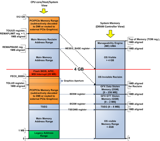
Figure 14 shows the Haswell system address map from the CPU core perspective and from the DRAM controller perspective. System address maps from both perspectives are different because the DRAM controller doesn't see memory ranges consumed by PCI/PCIe devices and it doesn't need such visibility either. The CPU views the memory ranges from TOLUD-to-4GB as allocated to PCI/PCIe devices, while the DRAM controller views the same memory range to be allocated to DRAM. Such different "views" are possible because the northbridge remaps the respective memory range in the DRAM from TOLUD-to-4GB (as seen from DRAM controller) to a new memory range above 4GB called "reclaim" memory range in the CPU memory space. The "reclaim" memory range is determined by two registers: REMAP BASE and REMAP LIMIT registers in the northbridge. The memory remapping logic in the northbridge carries out the remapping task, as you can see in Figure 13.
Boxes with light blue color in Figure 14 represent memory ranges occupied by RAM. This means that the DRAM controller sees the available RAM as a contiguous memory range while the CPU core doesn't. The CPU core view contains "holes" in the memory range below 4GB that don't belong to RAM—the "holes" are marked as boxes with non-light-blue colors in Figure 14.
Detail of the memory ranges in Figure 14 as follows:
- Legacy address range (as seen from CPU core perspective)—This range is the DOS compatibility range between 0-to-1MB. Memory transactions targeting the range between 0-640KB are always routed to DRAM, while memory transactions targeting the range between 640KB-1MB are routed based on the value of the PAM register which controls the respective ranges. Recall that there are seven PAM registers controlling the memory range between 640KB-1MB.
- Main memory ranges are memory ranges occupied by DRAM that don't require address remapping. OS has visibility to these ranges. The "normal" memory range logic in Figure 13 handles these memory ranges. These memory ranges have identical mappings from both the CPU perspective and the DRAM controller perspective.
- TSEG range—This memory range has an identical mapping from both the CPU perspective and the DRAM controller perspective. TSEG is an abbreviation for "top of main memory segment." However, in today's context this means the segment that lies in the top of main memory range below the 4GB limit. The start of this memory range is determined by the value of the TSEG memory base (TSEGMB) register in the hostbridge. Contents of this segment can only be seen when the CPU is running in system management mode (SMM). Therefore, code running outside of SMM doesn't have visibility of this range in RAM, even the operating system code. This segment stores the runtime data and code of the platform firmware.
- "GFX GTT Stolen" memory range—This memory range is seen as part of the PCI/PCIe memory range from the CPU perspective, while it's seen as part of the DRAM from DRAM controller perspective. This memory range only exists if the integrated graphics device (IGD) in the CPU is enabled in the hostbridge GMCH graphics control (GGC) register (via its VAMEN bit)—the platform firmware must initialize the bit based on the firmware configuration setting. This memory range stores the graphics translation table (GTT) entries—GTT entries are akin to page table entries (PTEs) in the CPU, but GTT entries are used for graphics memory. This memory range occupies the PCI/PCIe memory range from the CPU perspective despite the fact that it physically resides in the system memory (DRAM), not in the local RAM of a PCIe graphics card. Bits 8-9 (GGMS bits) in the GGC register in the hostbridge determine the size of this memory range, while the base of the GTT stolen memory (BGSM) register in the hostbridge determines the start/base address of this memory range.
- "GFX stolen" memory range—This memory range is seen as part of the PCI/PCIe memory range from the CPU perspective, while it's seen as part of the DRAM from the DRAM controller perspective. This memory range only exists if the IGD in the CPU is enabled—see "GFX GTT stolen" above for details on enabling the IGD. This memory range stores the graphics data, i.e., it acts as graphics memory for the IGD. This memory range occupies the PCI/PCIe memory range from the CPU perspective despite the fact that it physically resides in the system memory (DRAM), not in the local RAM of a PCIe graphics card. Bits 3-7 (GMS bits) in the GGC register in the hostbridge determine the size of this memory range, while the base data of stolen memory (BDSM) register in the hostbridge determines the start/base address of this memory range.
- PCI/PCIe memory range below 4GB—This memory range is only seen from the CPU perspective. This range is determined by whether the IGD is activated or not. If the IGD is active, this memory range starts at the value of the BGSM register; otherwise this memory range starts at the value of TOLUD register. The upper limit of this memory range is 4GB-20MB (FEC0_0000h). Access to this range is forwarded to either the external PCIe graphics via the PCIe 3.0 connection or to the southbridge via the DMI.
- PCI/PCIe memory range above 4GB—This memory range is only seen from the CPU perspective. The value of top of upper usable DRAM (TOUUD) register in the hostbridge determines the start of this memory range. The value of TOUUD is equal to the value of REMAPLIMIT register plus one. The PMLIMITU register (in the hostbridge) value determines the end of this memory range. Access to this range is forwarded to either the external PCIe graphics via the PCIe 3.0 connection or to the southbridge via the DMI.
- Graphics aperture range—This memory range is seen as part of PCI/PCIe memory range below 4GB in Figure 14. However, in practice, this memory range may as well reside in the PCI/PCIe memory range above 4GB, depending on the platform firmware and the system configuration. This memory range is always mapped to the PCI/PCIe memory range. It's used as contiguous address space or as additional graphics memory space if the graphics memory in the IGD or external PCIe graphics card is running out. The graphics aperture range in the platform firmware configuration must be enabled for this range to exist. Otherwise, it doesn't exist. Memory management for the system memory allocated to serve the graphics aperture uses a graphics translation table just like the legacy AGP aperture. The difference lies in the possibility that the aperture lies above the 4GB limit and the handling of the graphics aperture memory management. It's the responsibility of the OS—specifically the graphics device driver—to carry out memory management for the graphics aperture. Refer to the first part of this series for graphics aperture basics (at /system-address-map-initialization-in-x86x64-architecture-part-1-pci-based-systems/). The graphics memory aperture base address register (GMADR) in the IGD determines the start address of the graphics aperture when the IGD acts as the graphics chip in the Haswell platform.
- Flash BIOS, APIC, MSI interrupt memory range (FEC0_0000h - FFFF_FFFFh)—As explained in the previous section, all memory transactions targeting this compatibility memory range are always routed to the DMI interface, except those targeting the MSI address range and the APIC memory ranges that correspond to the local APIC in the CPU cores. Memory transactions targeting the last two ranges are always directed to the CPU.
- Main memory reclaim address range—This memory range occupies a different address when viewed from the CPU perspective and from the DRAM controller perspective. The REMAPBASE and REMAPLIMIT register in the hostbridge determine the start and the end of this memory range as seen from the CPU perspective. The TOLUD register and the 4GB limit defines the start and end of the same memory range when viewed from the DRAM controller perspective. The "remapped memory range logic" in the hostbridge—shown in Figure 13—remaps memory transactions from the CPU targeting this memory range before the transactions reach the DRAM controller.
- Manageability engine UMA memory range—This range is not controlled by the CPU. The manageability engine (ME) is integrated into the 8-series PCH (southbridge). The platform firmware reads the Intel management engine UMA Register in the 8-series PCH to determine the size of this range. The platform firmware must allocate this range from the top of memory (TOM) up-to the size requested by UMA register. The platform firmware initializes the MESEG_BASE and MESEG_MASK registers in the hostbridge to allocate the requested range from DRAM. ME is basically a microcontroller running in its own execution environment, out of the CPU's control. ME uses the manageability engine UMA memory range in RAM to cache its firmware while the system is not in low power state. ME uses its own—integrated—static RAM if the system is on low-power state. ME doesn't run when the system is completely out of power.
At this point, the Haswell system memory map should be clear. Nonetheless, we are going to look into a hypothetical memory read transaction to improve our Haswell system memory map understanding. Let's make the following assumptions on the system configuration:
- Physical memory (DRAM) size: 6GB
- Memory space allocated to memory mapped IO (including Flash, APIC, MSI, Intel TXT): 1GB
- Size of remapped physical memory: 1GB
- Top of memory (TOM): 1_8000_0000h (6GB)
- ME UMA size: 0 — ME is disabled
- TOUUD: 1_C000_0000h (7GB) — This address is 1MB-aligned
- TOLUD: C000_0000h (3GB)
- REMAPBASE: 1_8000_0000h (6GB)
- REMAPLIMIT: 1_BFF0_0000h (7GB - 1)
- Note: The remap range is inclusive of the base and limit addresses. In the address decoder, bits 0-19 of the remap base address are assumed to be 0h. Similarly, bits 0-19 of the remap limit are assumed to be 0Fh. This configuration ensures the remap range to stay in 1MB boundaries.
Now, let's trace a memory read transaction that targets 1_8000_0000h (6GB) physical address in this system configuration. Figure 15 shows how the memory read transaction travels in the system.
Figure 15. Haswell memory read transaction sample
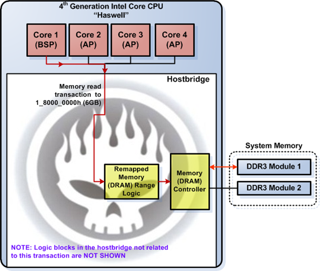
The red lines in Figure 15 denote the memory read transaction. Figure 15 intentionally doesn't show logic blocks not related to the memory read transaction to ease understanding of the transaction flow. Figure 15 shows the memory read transaction originated from CPU core 1. Then, the "remapped memory range logic" claims the memory read transaction once it enters the hostbridge because it's within the range covered by REMAPBASE and REMAPLIMIT registers. The "remapped memory range logic" then remaps the transaction target address into the address as seen from the DRAM controller perspective and forwards the transaction to the DRAM controller afterwards. The DRAM controller then handles the memory read transaction—i.e., it fetches the correct contents from the DRAM module.
The sample memory read transaction illustrates how the logic block in the hostbridge claims a memory read transaction and processes it accordingly. The Haswell system address map should be clear to you once you fully understand this memory read transaction sample.
Last but not least, you might be asking how the PCIe expansion ROM is addressed in Haswell. Well, it's very similar to a PCI-based system. The XROMBAR register in the particular PCIe expansion card must be enabled and programmed to consume memory range in the PCI/PCIe memory range. The rest is just the same as in a PCI-based system. There is no particular enhancement carried out by the PCIe bus protocol in this respect.
PCIe enhanced configuration space in Haswell platform
In this section we will look at PCIe enhanced configuration space location in the Haswell system address map. The first 256-byte PCIe configuration space registers are mapped to the CPU IO space at port CF8h-CFFh, just as in the legacy PCI bus—in addition, these registers are also mapped to the PCIe enhanced configuration space.
Contrary to legacy PCI configuration space, the entire PCIe configuration space (4KB per-device) is located in the CPU memory space. On the x86/x64 platform, the memory range consumed by the PCIe configuration space is relocatable in the CPU memory space. The platform firmware must initialize the location of this configuration space in the CPU memory space. We should look more closely into Haswell-specific implementation in this section.
Now, let's calculate the memory space requirement of the PCIe configuration space registers:
- The maximum number or PCIe buses in the system is 256
- The maximum number of PCIe devices per bus is 32
- The maximum number of function per device is 8
- Each function can implement up-to 4KB configuration registers
Using the statistics above, the entire PCIe configuration space registers requires: 256 x 32 x 8 x 4KB of memory space. This amounts to 256MB of memory space. Therefore, the platform firmware must initialize the system address map to accommodate this PCIe configuration space requirement. However, in practice, the memory space requirement of the PCIe enhanced configuration space in a particular system can be less than 256MB because the system cannot support that many PCIe devices physically.
In most cases, the PCIe enhanced configuration space is carved out of the PCI/PCIe memory range. The PCIe configuration space can be mapped to the PCI/PCIe memory range below 4GB (from TOLUD to the 4GB limit) or mapped to PCI/PCIe memory above the 4GB limit (above TOUUD) in the Haswell memory map, as shown in Figure 16.
On the Haswell platform, the PCI express register range base address (PCIEXBAR)—a register—in the hostbridge determines the location of the PCIe enhanced configuration space. PCIEXBAR contents determine the start address and the size of the PCIe enhanced configuration space. Figure 16 shows the two possible alternatives to map the PCIe enhanced configuration space. They are marked as "Mapping Alternative 1" (within the PCI/PCIe memory range below 4GB) and "Mapping Alternative 2" (within the PCI/PCIe memory range above TOUUD). PCIEXBAR can set the size of the PCIe enhanced configuration space to 64 MB, 128 MB or 256 MB. The platform firmware should initialize the bits that control the size of the PCIe enhanced configuration space in PCIEXBAR at boot.
Figure 16. PCIe enhanced configuration space register mapping on Haswell platform
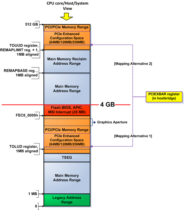
Mapping of the PCIe enhanced configuration space to the Haswell system address map should be clear at this point. Now, let's proceed to learn how to access the PCIe enhanced configuration space register. The memory address used to access the PCIe configuration space of a specific device function on the Haswell platform follows:
PCIe_reg_addr_in_CPU_memory_space = PCIEXBAR + Bus_Number * 1MB +
Device_Number * 32KB + Function_Number * 4KB +
Register_Offset
Perhaps you're asking where the 1MB, 32KB, and 4KB multipliers come from. It's simple actually: For each bus, we need 32 (device) * 8 (function) * 4KB of memory space, this is equal to 1MB; for each device, we need 8 (function) * 4KB of memory space, this is equal to 32KB.
Now, let's look into a simple sample. Let's assume that PCIEXBAR is initialized to C000_0000h (3GB) and we want to access the PCIe configuration register in Bus 0, device 2, function 1, at offset 40h. What is the address of this particular register? Let's calculate it:
Register_address_in_memory = C000_0000h + 0 * 1MB + 2 * 32KB + 1 * 4KB + 40h
Register_address_in_memory = C000_0000h + 0 + 1_0000h + 1000h + 40h
Register_address_in_memory = C001_1040h
We found that the target PCIe configuration register is located at C001_1040h in the CPU memory space. With this sample, you should now have no problem dealing with PCIe enhanced configuration space.
System Management Mode (SMM) memory on the Haswell platform
In the first article of this series, you learned that there are two memory ranges used to store SMM code and data, the high segment (HSEG) and TSEG. However, on the Haswell platform, HSEG has been deprecated and unsupported. Therefore, there is only one memory range used to store SMM code and data in Haswell, the TSEG memory range.
Figure 14 shows the location of the SMM memory in the system address map. The TSEGMB register in the hostbridge controls the TSEG start address. The TSEG memory range always ends at the value of BGSM register. Contents of the TSEG memory range are only accessible in two occasions. The first is when the system has just started and the platform firmware has not initialized the TSEG configuration. The second is when the CPU is running in system management mode. Access to TSEG is controlled by the system management RAM control (SMRAMC) register in the hostbridge.
The Haswell hostbridge prevents access not originating in the CPU core to TSEG. This prevents "rogue" hardware or firmware code running on add-on device to mess with contents of TSEG. The main reason to do this is because the security of the system is compromised if a device other than the CPU is given access to TSEG. At this point, everything regarding SMM memory in a typical Haswell-based system should be clear.
Graphics Address Remapping/Relocation Table (GART) on Haswell platform
In this section we are going to delve into GART. In the first article, I talked about GART in a legacy system, i.e. AGP GART. This section talks about present-day GART, i.e., GART in a PCIe-based system. Microsoft outlines requirements for GART implementation in a PCIe-based system—PCIe GART for short. You can read the requirements at http://msdn.microsoft.com/en-us/library/windows/hardware/gg463285.aspx. This is the relevant excerpt:
By definition, AGP requires a chipset with a graphics address relocation table (GART), which provides a linear view of nonlinear system memory to the graphics device. PCIe, however, requires that the memory linearization hardware exist on the graphics device itself instead of on the chipset. Consequently, driver support for memory linearization in PCIe must exist in the video driver, instead of as an AGP-style separate GART miniport driver. Graphics hardware vendors who want to use nonlocal video memory in their Windows XP driver model (XPDM) drivers must implement both memory linearization hardware and the corresponding software. All PCIe graphics adapters that are compatible with the WDDM must support memory linearization in hardware and software."
It's clear from the excerpt above that GART logic must be implemented in the PCIe graphics chip itself, not in the chipset logic. However, in the case of Haswell, there is an integrated PCIe graphics chip—the IGD—which is part of the northbridge. This is not a problem, though, as long as the integrated PCIe graphics implements its GART logic, i.e., the GART logic is part of the IGD, not part of other logic in the northbridge. This way the system is compliant with the Microsoft requirement above. Indeed, Haswell implement the GART logic as part of the IGD. We'll look closer into it in this section.
Figure 17. Haswell GART implementation
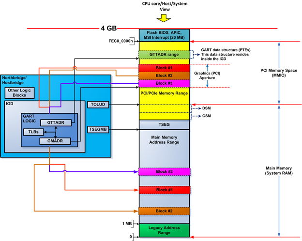
Figure 17 shows the inner working of the GART logic in the IGD, which is located inside the northbridge/hostbridge. Figure 17 shows that the GART logic maps three memory blocks in the graphics aperture—located in the PCI/PCIe memory range—to three different memory blocks in the main memory (system DRAM).
I'd like to point out the meaning of the abbreviations and component naming related to GART shown in Figure 17, before we get into details of the GART logic. These are the details:
- IGD or internal graphics device is the integrated graphics chip of the Haswell platform. This chip is integrated in to the CPU silicon die. This chip contains the GART logic.
- GTTADR is the graphics translation table base register. This register contains the start address of the graphics translation table, i.e., the start of the GART entries in the CPU memory space. Figure 17 shows the GART entries reside in the GTTADR range (marked in light green). The GTTADR range is a memory-mapped IO range because the contents of the range reside in a PCIe device, the IGD device. This memory range is not located in system memory but in the IGD. You can think of it as a buffer (memory) containing GART entries but residing in the IGD. This is different from GART entries in a legacy AGP system, where the GART entries reside in system memory.
- GMADR is the graphics memory aperture base register. This register is part of the GART logic. Contents of this register contain the start address of the graphics aperture in the CPU memory space. Figure 17 shows that GMADR points to start of Block #1, which is the first block of the graphics aperture range.
- TLBs are the translation look-aside buffers used to handle graphics memory transactions. They are part of the GART logic in the IGD. These TLBs are similar to TLBs you would find in the CPU's memory management unit (MMU).
- PTEs means page table entries. I use this term to highlight the fact that the GART entries are basically similar to PTEs in the CPU but these are used specifically for graphics.
- DSM is the graphics data stolen memory. This is the memory range used by the IGD as graphics memory. If you look at Figure 14, this range is part of the PCI/PCIe memory range despite it resides in the system DRAM. It resides in system DRAM because it's below TOLUD. This memory range is only accessible to the IGD at runtime. Therefore, it behaves just like external PCIe graphics card local memory.
- GSM is the graphics translation table (GTT) stolen memory. This memory range is completely different from the range covered by GTTADR. This memory range contains GTT entries for IGD internal use only. GTT entries in this memory range are not the same as GTT entries for GART. You have to pay attention to this difference.
- TOLUD is the top of low usable DRAM register. This register contains the highest address below 4GB that's used by the system DRAM.
- TSEGMB is the TSEG memory base register. This register contains the start address of TSEG.
- Graphics aperture is a memory range in the CPU memory address space which is part of the PCI/PCIe memory space and is used to provide linear address space to additional graphics memory. This is actually very similar to the AGP aperture in legacy AGP-based systems, as explained in the first article. The only difference is the possible location of the graphics aperture. In legacy AGP-based system, the graphics aperture could only be located below 4GB, whereas the graphics aperture in PCIe-based system can lie either below 4GB or above 4GB, as long as it's within the PCI/PCIe memory range.
- Block #1, Block #2, Block #3. These blocks illustrate mapping of adjacent memory blocks from the graphics aperture range to the system DRAM memory range. They illustrate the presence of linear memory space in the graphics aperture range, which is translated by the GART logic into memory blocks allocated by the OS in the system DRAM. If you are still confused about how this mapping works out, read the GART section in the first article.
Figure 17 simplifies a couple of things; among them is the location of the graphics aperture memory range. The graphics aperture pointed to by GMADR can start anywhere in the CPU memory space, either below 4G or above 4GB. However, Figure 17 shows the graphics aperture memory range resides below 4GB. You have to be aware of this.
Let's summarize the difference between legacy AGP GART and modern-day PCIe GART. The first one is that AGP GART logic was implemented as part of the hostbridge while modern-day GART logic is implemented as part of the PCIe graphics chip. In case the PCIe graphics chip is located in the hostbridge (like in the Haswell case), the GART logic will be part of the hostbridge. The operating system treats AGP GART and PCIe GART differently. AGP GART has its own miniport driver, while the PCIe GART driver is part of the PCIe graphics device driver. The second major difference is in the location of the graphics aperture: In a legacy AGP system, the graphics aperture always resides below 4GB while the modern-day PCIe graphics aperture can lie either below 4GB or above 4GB.
At this point you should have a clear understanding of GART on the Haswell platform. Even if this section talks about GART in the IGD PCIe graphics chip, you should be able to understand GART implemented by add-on PCIe graphics card easily because its principle is just the same. The difference is only in the location of the graphics memory/buffer, which is basically very similar from the system address map standpoint.
Haswell system address map initialization
In this section we'll have a look at the Haswell system address map initialization. We're not going to dive into the minute detail of the initialization but just sufficiently deep to understand the whole process. There are several steps in the Haswell boot process that are parts of system address map initialization. They are as follows:
- Manageability engine (ME) initialization—ME initialization happens prior to platform firmware code execution. ME initializes the Intel management engine UMA register in the 8-series PCH to signal to the platform firmware how much space it requires in the system DRAM for use as the ME UMA memory region.
- Chipset initialization—In this step, the chipset registers is initialized, including the chipset base address registers (BARs). We are particularly interested in chipset BAR initialization because this initialization affects the system address map. There are two chipsets in the Haswell platform, the northbridge and the southbridge. The northbridge is part of the CPU—sometimes called the uncore part—and the southbridge is the 8-series PCH. There are many registers involved in the system address map that are part of the chipset, as you can see from the previous sections. TOLUD, TSEGMB, and TOUUD are just a few of them. However, most of these registers are not initialized before the size of the system DRAM is known. Therefore, most of them are initialized as part of or after main memory initialization.
- Main memory (RAM) initialization—In this step, the memory controller initialization happens. The memory controller initialization and RAM initialization happen together as complementary code, because the platform firmware code must figure out the correct parameters supported by both the memory controller and the RAM modules installed on the system and then initialize both of the components into the "correct" setup. The memory sizing process is carried out in this step. The memory sizing determines the size of system DRAM. This is mostly carried out by reading contents of the serial presence detect (SPD) chip in the DRAM module. However, most platform firmware also executes random read/write operations to the DRAM to determine whether the claimed size in the SPD is indeed usable. As for the algorithm of the random read/write, it depends on the particular platform firmware. Initialization of the BARs in the chipset such as MESEG_BASE, TOLUD, TOUUD, TSEGMB, etc. is also carried in this step after the actual size of the system DRAM is known.
- PCI/PCIe device discovery and initialization—In this step, PCI devices—by extension the PCIe devices and other devices connected to PCI-compatible bus—are detected and initialized. The devices detected in this step could be part of the chipset and/or other PCI devices in the system, either soldered to the motherboard or on the PCI/PCIe expansion slots. There are several resources assignments to the device happening in this step: IO space assignment, memory-mapped IO (MMIO) space assignment, IRQ assignment (for devices that requires IRQ), and expansion ROM detection and execution. The assignment of memory or IO address space happens via the use of BAR in the PCI/PCIe devices. Initialization of USB devices happens in this step as well because USB is a PCI bus-compatible protocol. Other non-legacy devices are also initialized in this step, such as SATA, SPI, etc. The PCIe GART logic registers initialization also happens in this step because all of them point to memory ranges in the PCI/PCIe memory range. This step above actually consists of two sub-steps:
- Initialization of the critical PCI configuration space registers in all of the PCI and PCIe devices via the legacy PCI configuration mechanism that uses CPU IO port. This step is required because only the CPU IO port used for the initialization is hardcoded; thus, it can be used right away. This step also includes the step to initialize the PCIEXBAR in the hostbridge. The PCIe enhanced configuration space registers cannot be accessed before this register is initialized via legacy PCI configuration mechanism.
- Initialization of the PCIe enhanced configuration space registers—Once PCIEXBAR is initialized and the PCIe devices identified, the platform firmware can initialize all of the PCIe configuration registers, including the PCIe enhanced configuration space registers.
Once all of the registers in the hostbridge, the 8-series PCH, and all PCI and PCIe devices are initialized, the system address map is formed. The code in the Haswell platform firmware that carries out this initialization must be complicated because, as you have seen in the "Haswell System Address Map" section, the system address map is complicated. However, at this point you should have a clear understanding of a modern-day PCIe-based system from system address map point of view, including initialization of the system address map—carried out by the platform firmware.
Deeper look into UEFI GetMemoryMap() interface
In the first part of this series, you learned about the BIOS E820h interface. In this article I would only reiterate the UEFI equivalent of that function, the UEFI GetMemoryMap() function. This function is available as part of the UEFI boot services. Therefore, you need to traverse into the UEFI boot services table to "call" the function. The "simplified" algorithm to call this function as follows:
The GetMemoryMap() function returns a similar data structure to the one returned by the legacy E820h interface. The data structure is called EFI_MEMORY_DESCRIPTOR. EFI_MEMORY_DESCRIPTOR is defined as follows:
//*******************************************************
//EFI_MEMORY_DESCRIPTOR
//*******************************************************
typedef struct {
UINT32 Type;
EFI_PHYSICAL_ADDRESS PhysicalStart;
EFI_VIRTUAL_ADDRESS VirtualStart;
UINT64 NumberOfPages;
UINT64 Attribute;
} EFI_MEMORY_DESCRIPTOR;
The GetMemoryMap() function returns a copy of the current memory map. The map is an array of memory descriptors, each of which describes a contiguous block of memory. The map describes all of memory, no matter how it is being used. The memory map is only used to describe memory that is present in the system. Memory descriptors are never used to describe holes in the system memory map.
Well, this article doesn't try to delve deeper into UEFI GetMemoryMap() interface. You can read details of the interface and the EFI_MEMORY_DESCRIPTOR in the UEFI specification. Should you be interested in digging deeper, the GetMemoryMap() function is located in the "Boot Services" chapter of the UEFI specification, under the "Memory Allocation Services" section.

Become a certified reverse engineer!
Closing thoughts
This article delves quite deeply into the Haswell system address map and its initialization. It should give strong background knowledge for those looking to understand present-day systems, which could be even more complex than the one explained here. If there is anything really intriguing regarding the Haswell platform, it's the manageability engine (ME). This part of the system deserves its own scrutiny and further research. I'm aware of at least one proof-of-concept work in this particular field, but it was not on Haswell.


