X86 Assembly Language, Part 3.2 [Updated 2019]
- Ge! Stop! What's Segmentation?
Memory segmentation
-
The 80186 is a faster version of the 8086. It also has a 20-bit address bus and 16-bit data bus, but has an improved instruction set. The 80186 was never widely used in computer systems.
-
The real successor to the 8086 is the 80286, which was introduced in 1982. It has a 24-bit address bus, which implies 16MB of memory address space. The data bus is still 16-bits wide, but the 80286 has some memory protection capabilities. It introduced the protected-mode into the IA architecture. Segmentation in this new mode is different from the real-mode segmentation. We present details on this new segmentation later. The 80286 is backward compatible in that it can run the 8086-based software.
- Huh, what's protected mode? And how many modes can the processor run on?
And what is backward compatibility?
Each processor introduced into the Intel family since the 8086 has been backward-compatible with earlier processors. This approach enables older software to run (without recompilation) on newer computers without modification. Newer software eventually appeared, requiring features of more advanced processors.
Intro to x86 Disassembly
-
Intel introduced its first 32-bit processor —the 80386— in 1985. It has a 32-bit data bus and 32-bit address bus. It follows their 32-bit architecture known as IA-32. The memory address space has grown substantially (from 16MB address space to 4GB). This processor introduced paging into the IA architecture. It also allowed definition of segments as large as 4GB. This effectively allowed for a "flat" model (i.e., effectively turning off segmentation). Later sections present details on this aspect. Like the 80286, it can run all the programs written for 8086 and 8088 processors.
What is paging?
Paging is a special job that microprocessors can perform to make the available amount of memory in a system appear larger and more dynamic than it actually is. In a paging system, a certain amount of space may be laid aside on the hard drive (or on any secondary storage) called the swap file or swap partition. The virtual memory of the system is everything a program can access like memory, and includes physical RAM and the swap space.
Eh! Flat model, what on earth could that mean? What other models can the memory operate on?
-
The Intel 80486 processor was introduced in 1989. This is an improved version of the 80386. While maintaining the same address and data buses, it combined the co-processor functions for performing floating point arithmetic. The 80486 processor has added more parallel execution capability to decode instructions and execution units to achieve a scalar execution rate of one instruction per clock. It has an 8KB on chip LI cache. Furthermore, support for the L2 cache and multiprocessing has been added. Later versions of the 80486 processors incorporated features such as energy saving mode for notebooks.
What is floating point arithmetic?
It is a function which handles all mathematical operations that have anything to do with floating point numbers or fractions. It is a dedicated logic unit specifically designed to work on floating point numbers and nothing else, hence the name. It can be defined as a specialized coprocessor that can manipulate numbers quicker than the basic microprocessor circuitry itself.
Instruction per what?!!
-
The latest in the family is the Pentium series. It is not named 80586 because Intel found belatedly that numbers couldn't be trademarked! The first Pentium was introduced in 1993.
-
The Pentium is similar to the 80486, but uses a 64-bit wide data bus. Internally, it has 128 and 256 bit wide data paths to speed up internal data transfers. However, the Pentium instruction set supports 32-bit operands like the 80486 processor. It has added a second execution pipeline to achieve superscalar performance by having the capability to execute two instructions per clock. It has also doubled the on chip LI cache, with 8KB for data and another 8KB for the instructions. Branch prediction has also been added. The Pentium Pro processor has a three-way superscalar architecture. That is, it can execute three instructions per clock cycle. The address bus has been expanded to 36bits, which gives it an address space of 64GB. It also provides dynamic execution including out-of-order and speculative execution. In addition to the LI caches provided by the Pentium, the Pentium Pro has a 256KB L2 cache in the same package as the CPU.
-
The Pentium II processor has added multimedia (MMX) instructions to the Pentium Pro architecture. It has expanded the LI data and instruction caches to 16KB each. It has also added more comprehensive power management features including Sleep and Deep Sleep modes to conserve power during idle times.
What are multimedia MMX instructions?
-
The Pentium III processor introduced streaming SIMD extensions (SSE), cache prefetch instructions, and memory fences, and the single-instruction multiple-data (SIMD) architecture for concurrent execution of multiple floating-point operations. Pentium 4 enhanced these features further.
What is SIMD?
-
Intel's 64-bit Itanium processor is targeted for server applications. For these applications, the 32-bit memory address space is not adequate. The Itanium uses a 64-bit address bus to provide substantially larger address space. Its data bus is 128 bits wide. In a major departure, Intel has moved from the CISC designs used in their 32-bit processors to RISC orientation for their 64-bit Itanium processors. The Itanium also incorporates several advanced architectural features to provide improved performance for the high-end server market.
What is the difference between RISC and CISC?
RISC and CISC stand for two different competing philosophies in designing modern computer architecture. The debate between them has been going on for a long time and will likely continue. The difference between RISC and CISC can lie on many levels.
CISC, pronounced sisk, stands for "Complex Instruction Set Computer". What is a complex instruction? For example, adding two integers is considered a simple instruction. But an instruction that copies an element from one array to another and automatically updates both array subscripts is considered a complex instruction.
The philosophy behind CISC is that hardware is always faster than software, therefore one should make a powerful instruction set, which provides programmers with assembly instructions to do a lot with short programs. In fact, in CISC architecture, what you do is just keep layering on more & more instructions. You get some new things that you find a lot of people are doing frequently, like the compiler always needs to generate; and we say, you know, let's put all that sequence of instructions in one single complex instruction. For instance, Intel and AMD CPUs are based on CISC architectures.
The other major architecture is RISC and stands for "Reduced Instruction Set Computer". This term is misleading; many are under the impression that there are fewer instruction in the processor's instruction set. You should realize that RISC actually means "(Reduced Instruction) Set Computer," not "Reduced (Instruction Set) Computer." That is, the goal of RISC was to reduce the complexity of individual instructions, not necessarily reduce the number of instructions a RISC CPU supports. RISC is sort of a push back against CISC when they just keep adding things
Most of the time, we're only doing this small subset of your RISC thing, and the compiler/writer still does not know yet how to use all these things and can't figure out how to generate, so we are gonna go ahead and try to figure out from HL code.

IBM PowerPC processors have RISC architecture. Apple Mac used to be based on PowerPC processors, but it is not true anymore. However, we can still find PowerPC processors in video game consoles like (Wii, Xbox 360, and PlayStation 3). Another RISC architecture is ARM, used extensively in consumer electronics, including:
- Mobile phones (Some Nokia and Sony Ericsson).
- Palms and Pocket-PCs PDAs, tablets, smartphones (Samsung galaxy, iPhones).
- Digital media and music players (iPodes).
- Calculators and computer peripherals such as hard drives and routers …
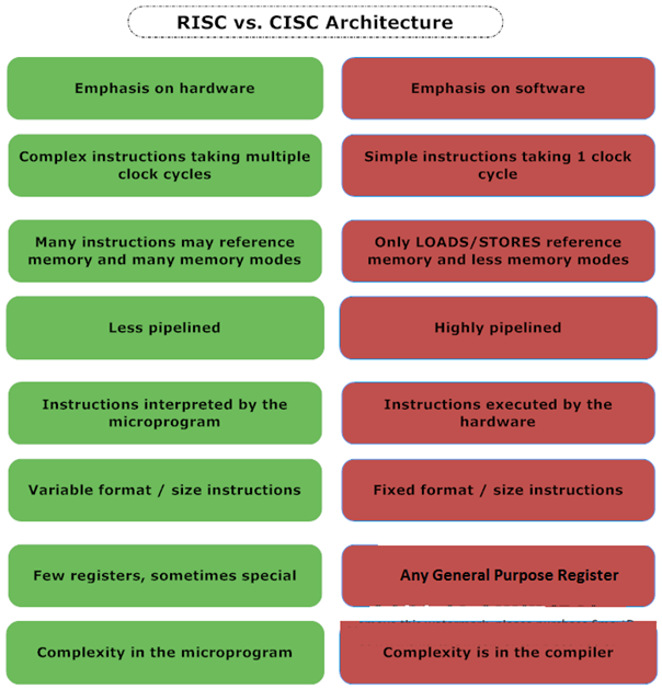
Here is a small additional side by side comparison between the two competing architectures:

And which one is better?
Right now this is still pretty much in the air. While the PC world is dominated by CISC processors, elsewhere mostly RISC processors are used.
But really now, which one is better?
It is just a matter of time. Some will claim that RISC is cheaper and faster, so it is the processor that will withstand the test of time, others say that RISC architecture puts too much of a burden on software, that the only way to go is to push the complexity to the hardware with CISC processors, as they are becoming faster and cheaper. Yet more and more I believe that RISC and CISC processors will someday merge because of the common goal of high performance.
That's the point, looking at the most modern processors, it becomes evident that the whole rivalry between CISC and RISC is now not of great importance. This is because the two architectures are converging closer to each other, with CPUs from each side incorporating ideas from the other.
-
Today's RISC chips support as many instructions as older CISC chips.
-
CISC chips are starting to use techniques there we associated with RISC chips.
Finally, you understand why the architecture is called x86 because the earliest processors in this family were identified by model numbers ending in the sequence "86″: the 8086, the 80186, the 80286, the 386, and the 486. Because one cannot establish trademark rights on numbers, Intel and most of its competitors began to use trademark-acceptable names such as Pentium for subsequent generations of processors, but the earlier naming scheme remains as a term for the entire family.
Registers
Most of the operations of the processor require processing data. Unfortunately, the slowest operations a processor can undertake are trying to read or write data in memory. As shown in first figure, when the processor accesses a data element, the request must travel outside of the processor, across the control bus, and into the memory storage unit. This process is not only complicated, but also forces the processor to wait while the memory access is being performed. This downtime could be spent processing other instructions.
To help solve this problem, the processor includes internal memory locations called registers. The registers are capable of storing data elements for processing without having to access the memory storage unit. The downside to registers is that a limited number of them are built into the processor chip. If you look carefully at the figure below, you should notice that the lower you go, the higher memory storage you get, but the slowest as well.

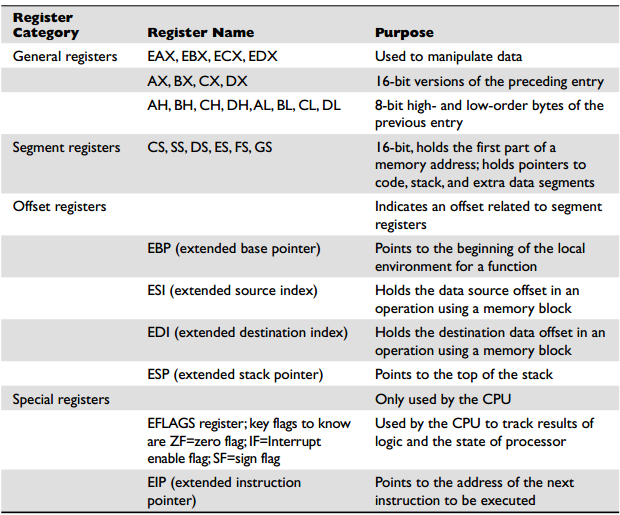
The IA-32 platform processors have multiple groups of registers of different sizes. They are classified according to the functions they perform. Different processors within the IA-32 platform include specialized registers. The core groups of registers available to all processors in the IA-32 family are shown in the following table.

Here we come to the end of our part 3. In the next tutorial, we will discuss the uses of registers in greater detail.
Intro to x86 Disassembly


